www.ti.com
ADS1x98ECG-FE Input Signals
33
SBAU171D–May 2010–Revised January 2016
Submit Documentation Feedback
Copyright © 2010–2016, Texas Instruments Incorporated
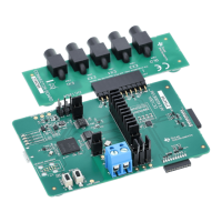
ADS1298ECG-FE/ADS1198ECG-FE
4.8.1 RLD Common Mode Voltage
The RLD common mode voltage can be set to (AVDD+AVSS)/2 or to an externally provided source. If the
application requires the common mode to be set to any voltage other than mid-supply, this can be
accomplished by setting the appropriate bit in the Configuration 3 Register. On the ADS1298ECG-FE, the
external RLDREF voltage is set using resistor R1 and adjustable resistor R2 (R1 and R2 are not installed
by default).
During power-up, the firmware configures the device for internal RLDREF operation. To configure the RLD
circuitry manually, use the following steps and the controls found on the ADC Register tab.
1. Verify that the Channel Input is set to the Normal Electrode mode for all channels (Channel
Registers tab).
2. In CONFIG3 control register (Channel Registers tab):
• Enable the RLD Buffer (RLD Buffer Power = Enable)
• Set the internal RLD reference (RLDREF Signal Source)
3. Select the electrodes for the RLD loop from the Right Leg Drive Derivation Control Registers controls
(LOFF and RLD tab)
Once these steps are completed, measure and verify that the voltage on either side of R38 is close to
mid-supply. This measurement confirms whether the RLD loop is functional.
The on-chip RLD signal can be fed back into the ADS1298 by shorting JP1. This RLD signal can then be
sent to the ADC (to measure for debug purposes) or to other electrodes for driving (to change the
reference drive in case the RL electrode falls off). Refer to the ADS1298 product data sheet or ADS1198
data sheet for additional details.
4.8.2 Driving the RLD Cable Shield
Apart from the RLD signal, the ADS1298ECG-FE also offers three options to drive the cable shield:
• In-phase RLD signal
• Out-of-phase RLD signal
• Board AGND
Table 4 summarizes the configuration of JP15 and JP17 for each of the options.
Table 4. RLD Jumper Options
ECG Cable
ELEC_SHD signal JP15 JP17
AGND 1-2 Don't Care
RLD (0: In phase) 2-3 2-3
RLD (180: Out of phase) 2-3 1-2
4.9 PACE Detection
The ADS1298 supports data rates up to 32kSPS for software PACE detection, which typically requires a
data rate of at least 8kSPS.
NOTE: The ADS1298ECG-FE does not include software PACE detection algorithms.
The ADS1298 provides the user the flexibility of doing hardware PACE detection with external circuitry.
PACE detection can be done simultaneously on two channels: one from the odd channels and one from
the even channels. Refer to the ADS1298 product data sheet or ADS1198 product data sheet for
additional details.
To turn on the PACE buffer and select the channels, set the PACE Register from the GPIO and OTHER
Registers tab. The PGA outputs of the selected channels are available at connector J5, pins 1 and 2.

 Loading...