KCU105 Board User Guide www.xilinx.com 26
UG917 (v1.4) September 25, 2015
Chapter 1: KCU105 Evaluation Board Features
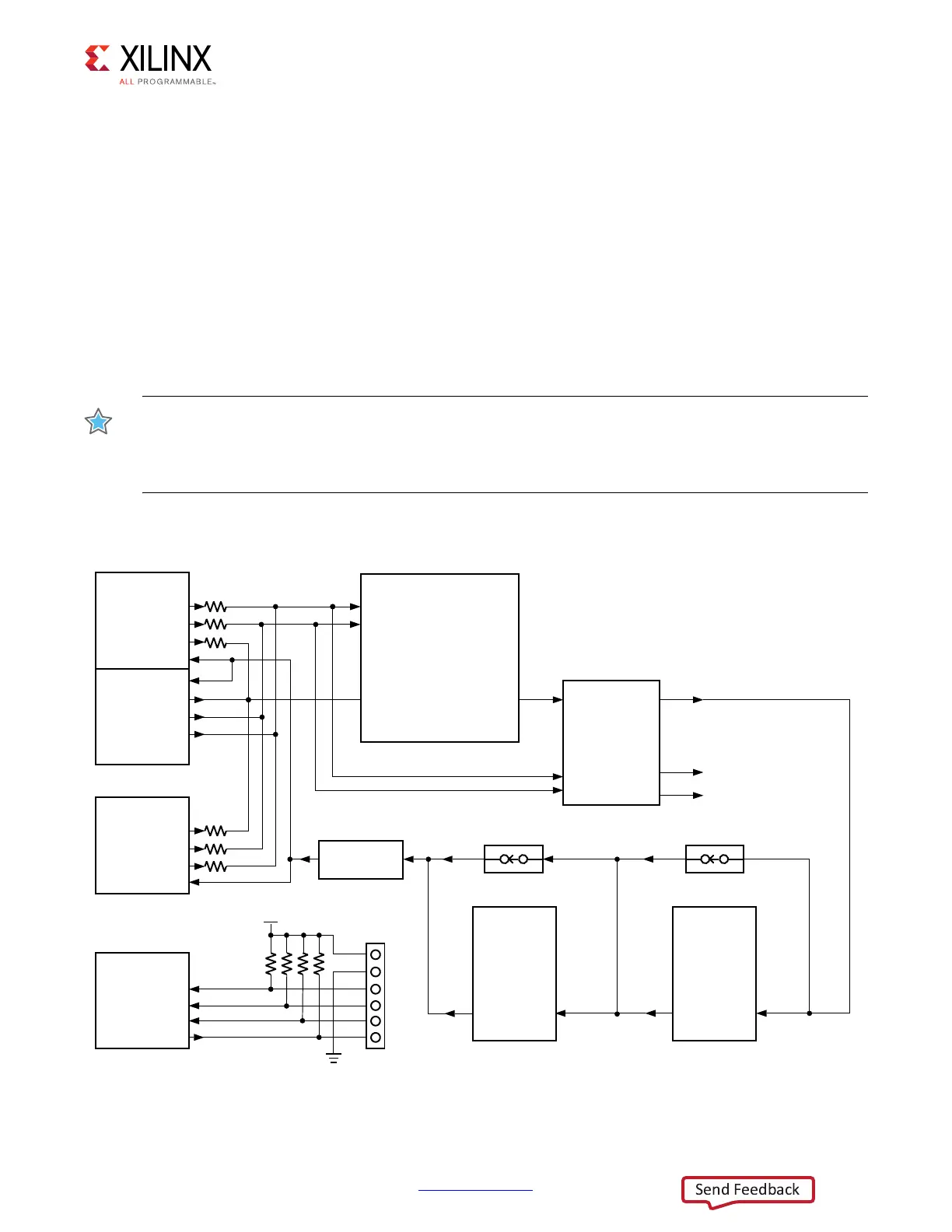
USB JTAG Interface
[Figure 1-2, callout 5]
JTAG configuration is provided through a Digilent onboard USB-to-JTAG configuration
logic module (U115) where a host computer accesses the KCU105 board JTAG chain through
a type-A (host side) to micro-B (KCU105 board side J87) USB cable.
A 2-mm JTAG header (J3) is also provided in parallel for access by Xilinx download cables
such as the platform cable USB II and the parallel cable IV. The JTAG chain of the KCU105
board is illustrated in Figure 1-8. JTAG configuration is allowed at any time regardless of
FPGA mode pin settings. JTAG initiated configuration takes priority over the configuration
method selected through the FPGA mode pin M2 (which is wired to SW15 pin 6, position 6).
IMPORTANT: The KCU105 board JTAG chain implementation supports up to 15 MHz TCK operation.
When using the Vivado Design Suite Hardware Manager to configure the KCU105 board, 15 MHz or
lower must be used for the TCK frequency setting. If the JTAG TCK is set to >15 MHz, the Vivado tools
display an unknown device instead of detecting the UltraScale Kintex KU040 device.
For more details about the Digilent USB JTAG Module, see the Digilent website [Ref 27].
X-Ref Target - Figure 1-8
Figure 1-8: JTAG Chain Block Diagram
'LJLOHQW
86%
0RGXOH
8
7&.
706
7',
7'2
-7$*
&RQ
-
7'2
7',
706
7&.
)3*$
8
7&.
706
7', 7'2
/HYHOVKLIWHG
9WR9
8
)0&/3&
&RQQHFWRU
-
7',7'2
)0&+3&
&RQQHFWRU
-
7',7'2
99
8
/HYHOVKLIWHGWR9
8 8
1& 1&
/HYHOVKLIWHGWR9
7R)0&+3&-
$QG)0&/3&-
6<6&7/5
;&=
8
%$1.
7',
706
7&.
7'2
6<6&7/5
;&=
8
%$1.
7&.
706
7',
7'2
6367%XV6ZLWFK 6367%XV6ZLWFK
7'2
7&.
706
-
*1'
6<6&7/5B7&.
6<6&7/5B706
6<6&7/5B7',
6<6&7/5B7'2
6<6B9
6\VWHP&RQWUROOHU8-7$*
8*BB

 Loading...


