RocketIO™ Transceiver User Guide www.xilinx.com 103
UG024 (v3.0) February 22, 2007
R
Chapter 3
Analog Design Considerations
Serial I/O Description
The RocketIO transceiver transmits and receives serial differential signals. This feature
operates at a nominal supply voltage of 2.5 VDC. A serial differential pair consists of a true
(V
P
) and a complement (V
N
) set of signals. The voltage difference represents the
transferred data. Thus: V
P
– V
N
= V
DATA
. Differential switching is performed at the
crossing of the two complementary signals. Therefore, no separate reference level is
needed. A graphical representation of this concept is shown in Figure 3-1.
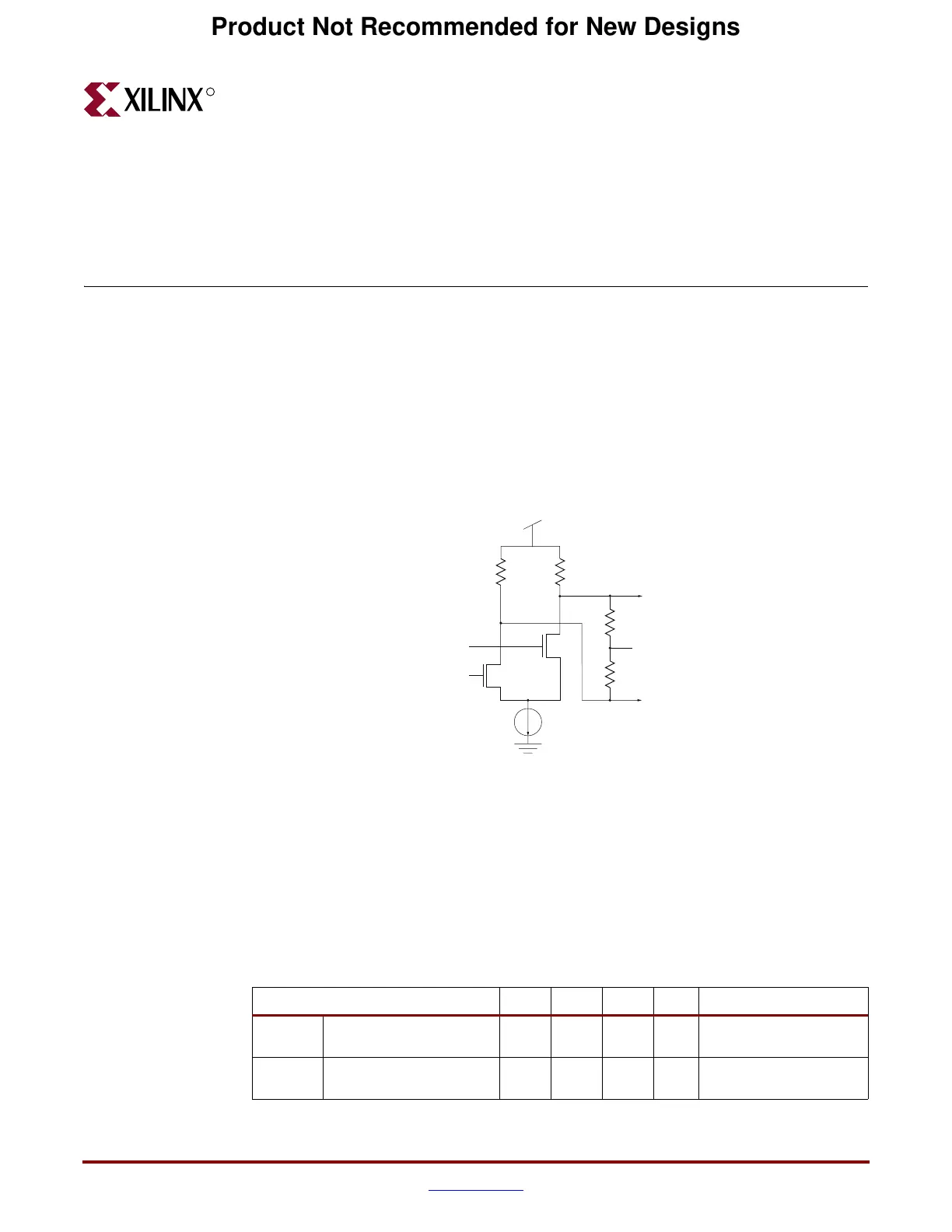
The RocketIO transceiver is implemented in Current Mode Logic (CML). A CML output
consists of transistors configured as shown in Figure 3-1. CML uses a positive supply and
offers easy interface requirements. In this configuration, both legs of the driver, V
P
and V
N
,
sink current, with one leg always sinking more current than its complement. The CML
output consists of a differential pair with 50Ω (or, optionally, 75Ω) source resistors. The
signal swing is created by switching the current in a common-drain differential pair.
The differential transmitter specification is shown in Table 3-1, page 103.
Figure 3-1: Differential Amplifier
Table 3-1: Differential Transmitter Parameters
Parameter Min Typ Max Units Conditions
V
OUT
Serial output differential
peak to peak (TXP/TXN)
800 1600 mV Output differential
voltage is programmable
V
TTX
Output termination
voltage supply
1.8 2.625 V
PMA
TXP
PMA
TXN
AVCCAUXTX
50Ω or 75Ω
50Ω or 75Ω
TXP pin
TXN pin
VTTX
Pullup
Network
GNDA
UG024_46_021704
Product Not Recommended for New Designs
 Loading...
