RocketIO™ Transceiver User Guide www.xilinx.com 41
UG024 (v3.0) February 22, 2007
Clocking
R
BREFCLK
At speeds of 2.5 Gb/s or greater, REFCLK configuration introduces more than the
maximum allowable jitter to the RocketIO transceiver. For these higher speeds, BREFCLK
configuration is required. The BREFCLK configuration uses dedicated routing resources
that reduce jitter.
BREFCLK must enter the FPGA through dedicated clock I/O. BREFCLK can connect to the
BREFCLK inputs of the transceiver and the CLKIN input of the DCM for creation of
USRCLKs. If all the transceivers on a Virtex-II Pro FPGA are to be used, two BREFCLKs
must be created, one for the top of the chip and one for the bottom. These dedicated clocks
use the same clock inputs for all packages:
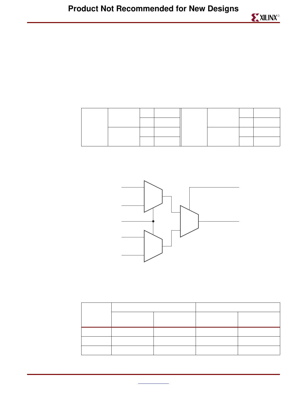
An attribute (REF_CLK_V_SEL) and a port (REFCLKSEL) determine which reference clock
is used for the MGT PMA block. Figure 2-1 shows how REFCLK and BREFCLK are
selected through use of REFCLKSEL and REF_CLK_V_SEL.
Table 2-3 shows the BREFCLK pin numbers for all packages. Note that these pads must be
used for BREFCLK operations.
Top
BREFCLK
PGCLK4S
Bottom
BREFCLK
PGCLK6P
NGCLK5P NGCLK7S
BREFCLK2
PGCLK2S
BREFCLK2
PGCLK0P
NGCLK3P NGCLK1S
Figure 2-1: REFCLK/BREFCLK Selection Logic
Table 2-3: BREFCLK Pin Numbers
Package
Top Bottom
BREFCLK
Pin Number
BREFCLK2
Pin Number
BREFCLK
Pin Number
BREFCLK2
Pin Number
FG256 A8/B8 B9/A9 R8/T8 T9/R9
FG456 C11/D11 D12/C12 W11/Y11 Y12/W12
FG676 B13/C13 C14/B14 AD13/AE13 AE14/AD14
0
0
0
1
1
1
1.5V
2.5V
REF_CLK_V_SEL
REFCLKSEL refclk_out
to PCS and PMA
refclk
refclk2
brefclk
brefclk2
ug024_35_091802
Product Not Recommended for New Designs
 Loading...
