38 www.xilinx.com RocketIO™ Transceiver User Guide
UG024 (v3.0) February 22, 2007
Chapter 1: RocketIO Transceiver Overview
R
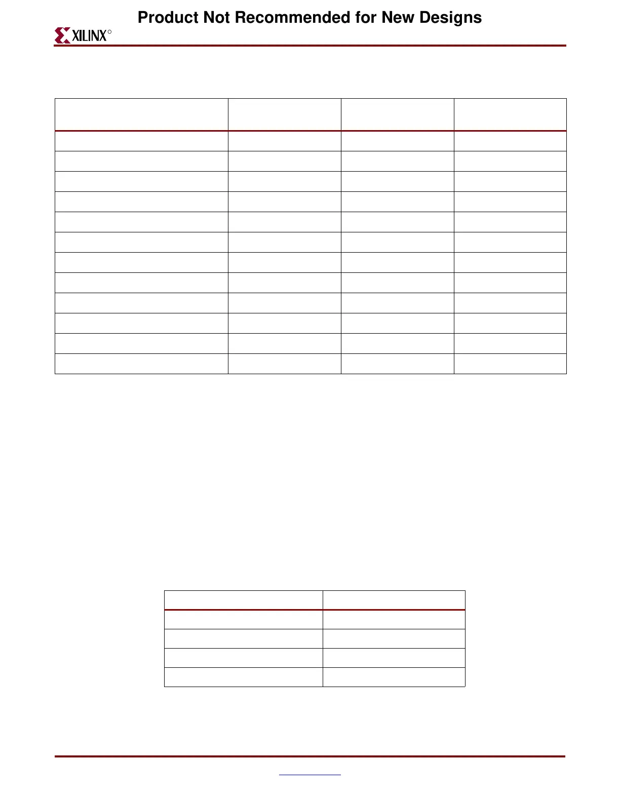
Byte Mapping
Most of the 4-bit wide status and control buses correlate to a specific byte of TXDATA or
RXDATA. This scheme is shown in Table 1-9. This creates a way to tie all the signals
together regardless of the data path width needed for the GT_CUSTOM. All other
primitives with specific data width paths and all byte-mapped ports are affected by this
situation. For example, a 1-byte wide data path has only 1-bit control and status bits
(TXKERR[0]) correlating to the data bits TXDATA[7:0]. Footnote 3 in Table 1-5 shows the
ports that use byte mapping.
RX_DECODE_USE TRUE TRUE TRUE
RX_LOS_INVALID_INCR 1
(1)
1
(1)
1
(1)
RX_LOS_THRESHOLD 4
(1)
4
(1)
4
(1)
RX_LOSS_OF_SYNC_FSM TRUE
(1)
TRUE
(1)
TRUE
(1)
SERDES_10B FALSE
(1)
FALSE
(1)
FALSE
(1)
TERMINATION_IMP 50
(1)
50
(1)
50
(1)
TX_BUFFER_USE TRUE TRUE TRUE
TX_CRC_FORCE_VALUE 11010110
(1)
11010110
(1)
11010110
(1)
TX_CRC_USE FALSE
(1)
FALSE
(1)
FALSE
(1)
TX_DATA_WIDTH N
(2)
N
(2)
N
(2)
TX_DIFF_CTRL 500
(1)
500
(1)
500
(1)
TX_PREEMPHASIS 0
(1)
0
(1)
0
(1)
Notes:
1. Modifiable attribute for specific primitives.
2. Depends on primitive used: either 1, 2, or 4.
3. CRC_EOP and CRC_SOP are not applicable for this primitive.
Table 1-8: Default Attribute Values: GT_FIBRE_CHAN, GT_INFINIBAND,
and GT_XAUI (Continued)
Attribute
Default
GT_FIBRE_CHAN
Default
GT_INFINIBAND
Default
GT_XAUI
Table 1-9: Control/Status Bus Association to Data Bus Byte Paths
Control/Status Bit Data Bits
[0] [7:0]
[1] [15:8]
[2] [23:16]
[3] [31:24]
Product Not Recommended for New Designs