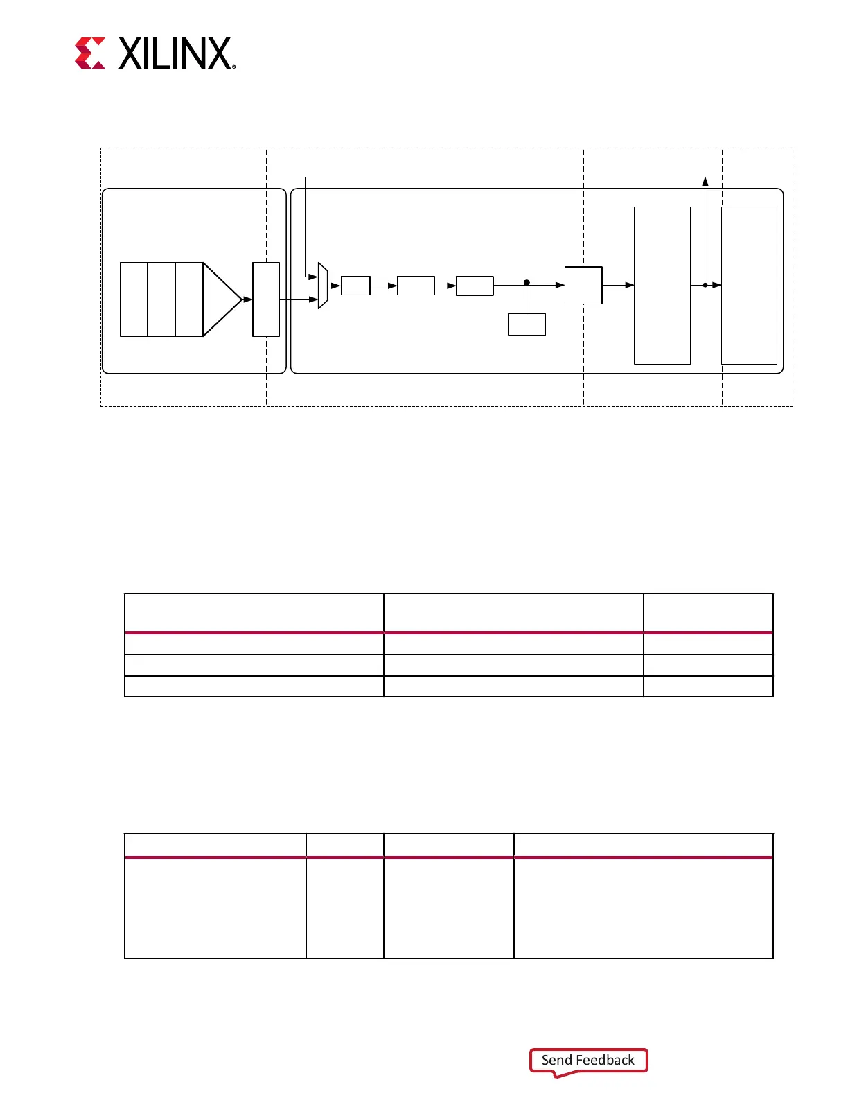
Figure 44: RX Clock Domains
RX Serial Clock
PMA Parallel Clock (XCLK) PCS Parallel Clock (RXUSRCLK)
Device Parallel Clock
(RXUSRCLK2)
Polarity
PRBS
Checker
FEC
Gray
Encoder
Pre-
Coder
RX PCS
DFE/
FFE
RX EQ ADC
RX PMA
To RX Parallel Data
(Near-End PCS Loopback)
From RX Parallel Data
(Far-End PCS Loopback)
RX
FIFO
SIPO
X20945-061418
RX
Interface
The GTM receiver includes an RX FIFO to support data width conversion when data crosses from
the XCLK to TXUSRCLK domain, and the table below shows the possible scenarios. The buer
does not tolerate ppm dierences and only provides phase compensaon between the two
clocks. The RX buer inside the GTM transceiver must always be used. Buer bypass is not
allowed.
Table 63: RX FIFO Data Width Conversion Scenarios
PMA Parallel Clock (XCLK) Domain
Data Width
PCS Parallel Clock (TXUSRCLK)
Domain Data Width
FEC Support
64-bit 64-bit No
128-bit 80-bit Yes
128-bit 128-bit No
Ports and attributes
The following table denes the RX buer ports.
Table 64: RX Buffer Ports
Port Dir Clock Domain Description
CH[0/1]_RXBUFSTATUS[1:0] Out RXUSRCLK RX buffer status:
Bit[1]: FIFO overflow status. A value of 1
indicates FIFO overflow.
Bit[0]: FIFO underflow status. A value of 1
indicates FIFO underflow.
Chapter 4: Receiver
UG581 (v1.0) January 4, 2019 www.xilinx.com
Virtex UltraScale+ GTM Transceivers 105
 Loading...
