RX CDR
The RX clock data recovery (CDR) circuit in each UltraScale+ FPGA GTM transceiver channel
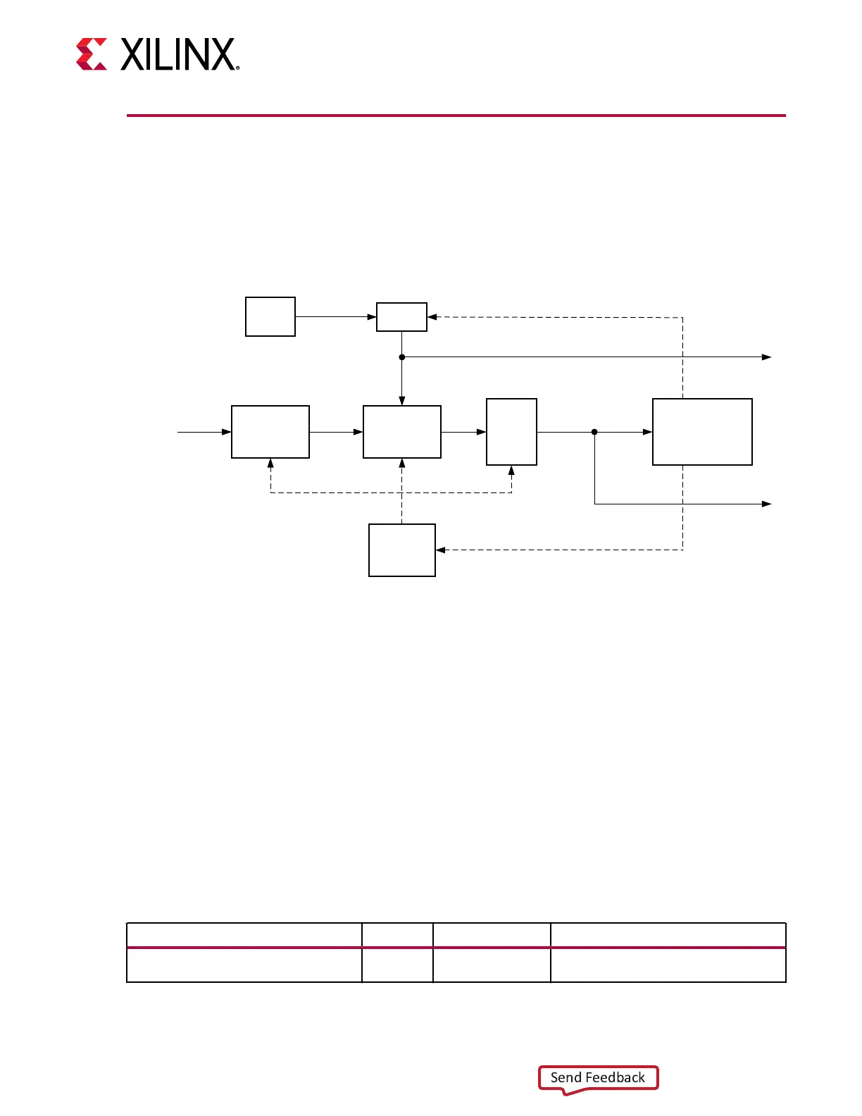
extracts the recovered clock and data from an incoming data stream. The following gure
illustrates the architecture of the CDR block. Clock paths are shown with doed lines for clarity.
Figure 40: CDR Block Diagram
Recovered
Clock
CTLE ADC
DFE
+
FFE
CDR FSM
RX Data
PI
Adaptation
PLL
RXP/N
X20925-053118
The GTM transceiver employs the baud-rate phase detecon CDR architecture. Incoming data
rst goes through receiver equalizaon and ADC where the data is sampled. The sampled data
then moves through FFE and DFE before feeding to the CDR state machine and the downstream
transceiver blocks.
The LCPLL provides a base clock to the phase interpolator. The phase interpolator in turn
produces ne, evenly spaced sampling phases to allow the CDR state machine to have ne phase
control. The CDR state machine can track incoming data streams that can have a frequency
oset from the local PLL reference clock.
Ports and Attributes
The following table denes the CDR ports.
Table 52:
CDR Ports
Port Dir Clock Domain Description
CH[0/1]_RXCDROVRDEN In Async Reserved. Use the recommended value
from the Wizard.
Chapter 4: Receiver
UG581 (v1.0) January 4, 2019 www.xilinx.com
Virtex UltraScale+ GTM Transceivers 93
 Loading...
