Chapter 5
Board Design Guidelines
This chapter presents topics related to implemenng a design on a printed circuit board that uses
GTM transceivers. GTM transceivers are analog circuits that require special consideraon and
aenon when designing and implemenng on a printed circuit board. Besides an understanding
of the funconality of the device pins, a design that performs opmally requires aenon to
issues such as device interfacing, transmission line impedance and roung, power supply design
ltering and distribuon, component selecon, and PCB layout and stackup design.
Pin Description and Design Guidelines
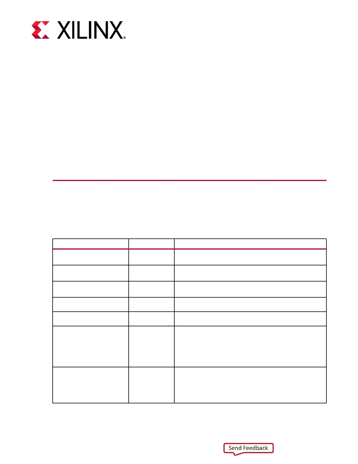
The following table denes the GTM transceiver Dual pins.
Table 73: GTM Transceiver Dual Pin Descriptions
Pins Dir Description
MGTREFCLKP
MGTREFCLKN
In/Out(Pad) Configured as either reference clock input pins or as RX recovered
clock output pins for the Dual.
MGTMRXP[1:0]
MGTMRXN[1:0]
In(Pad) RXP and RXN are the differential input pairs for each of the
receivers in the GTM transceiver Dual.
MGTMTXP[1:0]
MGTMTXN[1:0]
Out(Pad) TXP and TXN are the differential output pairs for each of the
transceivers in the GTM transceiver Dual.
MGTAVTTRCAL In(Pad) Bias current supply for the termination resistor calibration circuit.
See Termination Resistor Calibration Circuit.
MGTRREF In(Pad) Calibration resistor input pin for the termination resistor
calibration circuit. See Termination Resistor Calibration Circuit.
MGTAVCC In(Pad) MGTAVCC is the analog supply for the internal analog circuits of
the GTM transceiver Dual tile. This includes the analog circuits for
the PLL, transmitters, and receivers. Most packages have multiple
groups of power supply connections in the package for MGTAVCC.
Refer to the package pin definitions to identify the location of the
power supply group for a specific GTM transceiver Dual.The
nominal voltage is 0.9 VDC.
MGTAVTT
In(Pad) MGTAVTT is the analog supply for the transmitter and receiver
termination circuits of the GTM transceiver Dual tile. Most
packages have multiple groups of power supply connections in the
package for MGTAVTT. Refer to the package pin definitions to
identify the location of the power supply group for a specific GTM
transceiver Dual. The nominal voltage is 1.2 VDC.
UG581 (v1.0) January 4, 2019 www.xilinx.com
Virtex UltraScale+ GTM Transceivers 117
 Loading...
