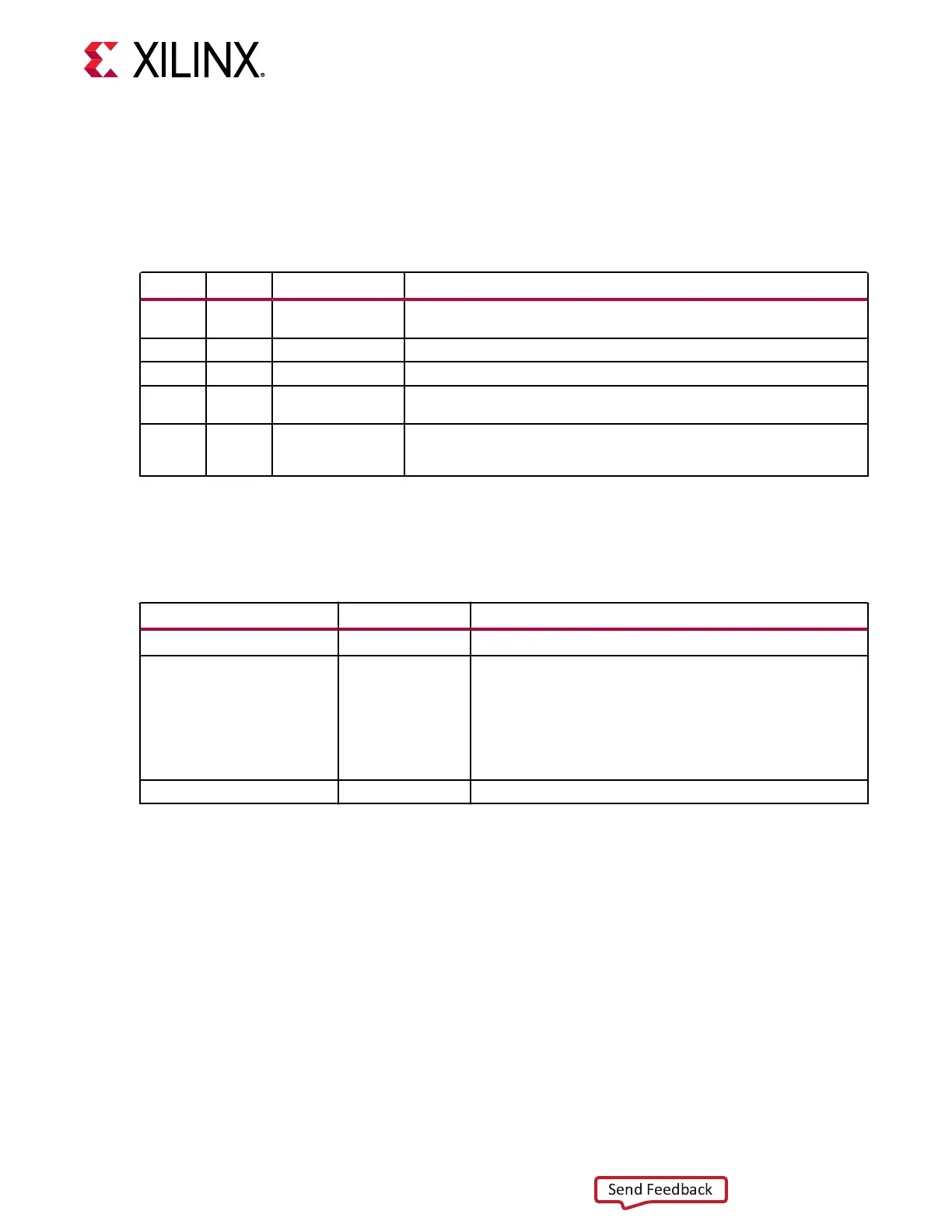
Ports and Attributes
The following table denes the reference clock input ports in the IBUFDS_GTM soware
primive.
Table 3: Reference Clock Input Ports (IBUFDS_GTM)
Port Dir Clock Domain Description
CEB In N/A This is the active-Low asynchronous clock enable signal for the clock buffer.
Setting this signal High powers down the clock buffer.
I In (pad) N/A These are the reference clock input ports that get mapped to GTREFCLKP.
IB In (pad) N/A These are the reference clock input ports that get mapped to GTREFCLKN.
O Out N/A This output drives the GTREFCLK signal in the GTM_DUAL software primitive.
Refer to Reference Clock Selection and Distribution for more details.
ODIV2 Out N/A This output can be configured to output either the O signal or a divide-by-2
version of the O signal. It can drive the BUFG_GT via the HROW routing. Refer
to Reference Clock Selection and Distribution for more details.
The following table denes the aributes in the IBUFDS_GTM soware primive that congure
the reference clock input.
Table 4: Reference Clock Input Attributes (IBUFDS_GTM)
Attribute Type Description
REFCLK_EN_TX_PATH 1-bit Reserved. This attribute must always be set to 1'b0.
REFCLK_HROW_CK_SEL 2-bit Configures the ODIV2 output port:
2'b00: ODIV2 = O.
2'b01: ODIV2 = Divide-by-2 version of O.
2'b10: ODIV2 = 1'b0.
2'b11: ODIV2 = Reserved.
REFCLK_ICNTL_RX
2-bit Reserved. Use the recommended value from the Wizard.
Output Mode
The reference clock output mode can be accessed via the OBUFDS_GTM soware primive. The
reference clock output mode structure for the OBUFDS_GTM primive is shown in the following
gure. The ports and aributes controlling the reference clock output are ed to the
OBUFDS_GTM soware primive.
Chapter 2: Shared Features
UG581 (v1.0) January 4, 2019 www.xilinx.com
Virtex UltraScale+ GTM Transceivers 13
 Loading...
