Ports and Attributes
The following table shows the DRP related ports for the GTM_DUAL.
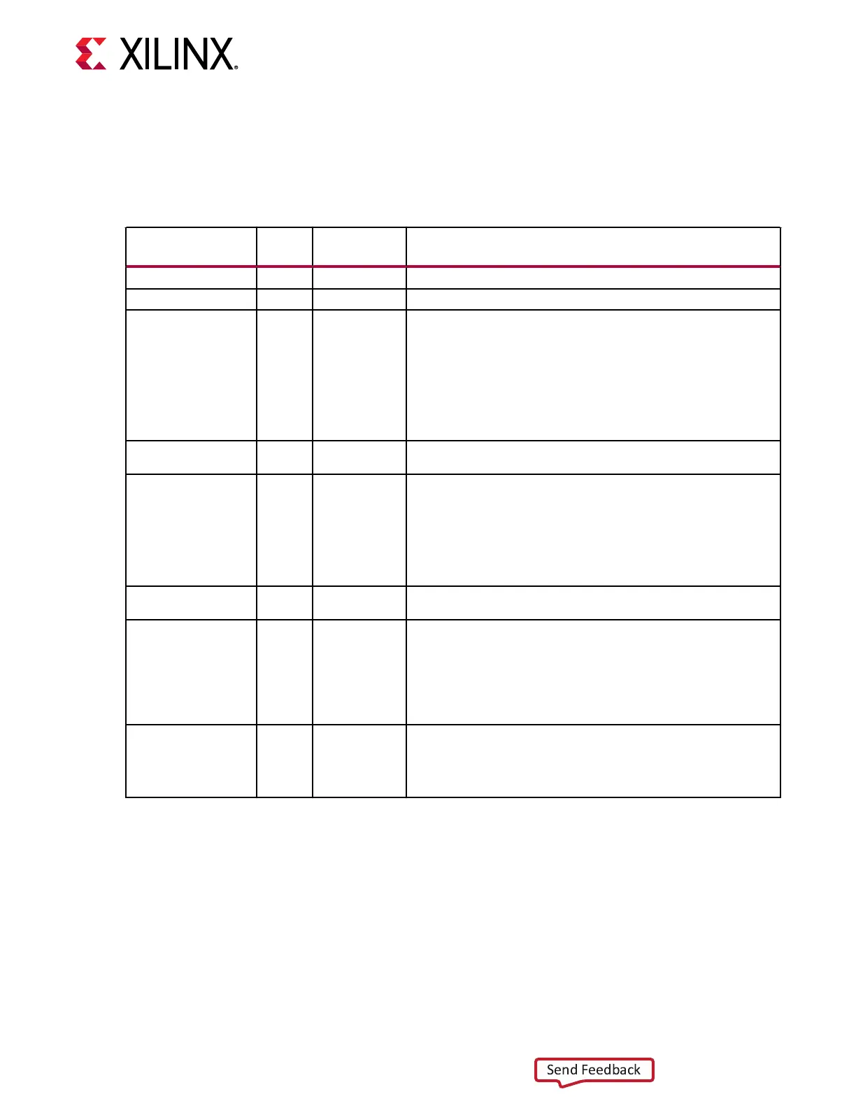
Table 25: DRP Ports of GTM_DUAL
Port Dir
Clock
Domain
Description
DRPADDR[10:0] In DRPCLK DRP address bus.
DRPCLK In N/A DRP interface clock.
DRPEN In DRPCLK DRP enable signal.
0: No read or write operation performed.
1: Enables a read or write operation.
For write operations. DRPWE and DRPEN should be driven High for
one DRPCLK cycle only. See Figure 22 for correct operation. For read
operations, DRPEN should be driven High for one DRPCLK cycle only.
See Figure 23 for correct operation.
DRPDI[15:0]
In DRPCLK Data bus for writing configuration data from the interconnect logic
resources to the transceivers.
DRPRDY Out DRPCLK Indicates operation is complete for write operations and data is valid
for read operations. If writing or reading a R/W register, DRPRDY
asserts six DRPCLK cycles after initiating a DRP transaction. For read-
only registers, the number of DRPCLK cycles for DRPRDY assertion
depends on the relationship between the DRPCLK frequency and the
USRCLK frequency. For read-only registers, if a DRPRDY is not seen
within 500 DRPCLK cycles after initiating a DRP transaction, reset the
DRP interface.
DRPDO[15:0]
Out DRPCLK Data bus for reading configuration data from the GTM transceiver to
the interconnect logic resources.
DRPWE In DRPCLK DRP write enable.
0: Read operation when DRPEN = 1.
1: Write operation when DRPEN is 1.
For write operations, DRPWE and DRPEN should be driven High for
one DRPCLK cycle only. See Figure 22 for correct operation.
DRPRST
In DRPCLK DRP reset. Reading read-only registers while the XCLK is not toggling
(e.g., during reset or change of reference clocks) causes the DRP to
not return a DRPRDY signal and prevent further DRP transactions. In
such an event, DRPRST must be pulsed to reset the DRP interface
before initiating further DRP transactions.
Usage Model
Write Operation
The following gure shows the DRP write operaon ming. New DRP operaons can be iniated
when DRPRDY is asserted.
Chapter 2: Shared Features
UG581 (v1.0) January 4, 2019 www.xilinx.com
Virtex UltraScale+ GTM Transceivers 48
 Loading...
