IEC05000748_2_en.vsd
UN ST1
TR1
ST2
TR2
START
TRIP
Comparator
UN > U1>
Start
t2
tReset2
&
Trip
Output
Logic
Step 2
Phase 1
Phase 1
Time integrator
tIReset2
ResetTypeCrv2
START
Start
t1
tReset1
&
Trip
Output
Logic
Step 1
Time integrator
tIReset1
ResetTypeCrv1
Comparator
UN > U2>
START
TRIP
TRIP
OR
OR
IEC05000748 V2 EN-US
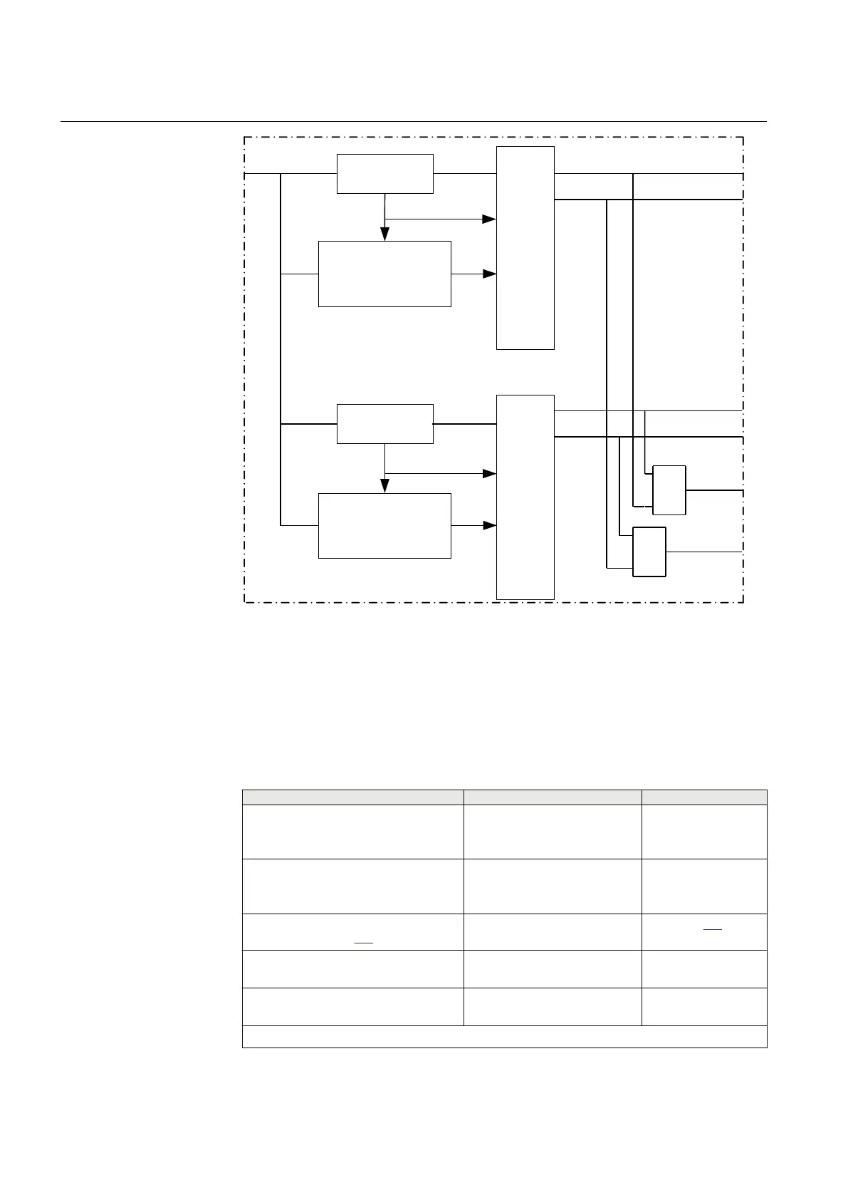
Figure 149: Schematic design of Two step residual overvoltage protection
ROV2PTOV
8.3.8 Technical data
M13317-2 v14
Table 160: ROV2PTOV technical data
Function
Range or value Accuracy
Operate voltage, step 1 - step 2 (1.0-200.0)% of
UBase
± 0.5% of U
r
at U ≤
U
r
± 0.5% of U at U > U
r
Absolute hysteresis (0.0–50.0)% of
UBase
± 0.5% of U
r
at U ≤
U
r
± 0.5% of U at U > U
r
Inverse time characteristics for low and
high step, see table 684
- See table 684
Definite time delay low step (step 1) at 0
to 1.2 x U
set
(0.00–6000.00) s ± 0.2% or ± 45 ms
whichever is greater
Definite time delay high step (step 2) at 0
to 1.2 x U
set
(0.000–60.000) s ± 0.2% or ± 45 ms
whichever is greater
Table continues on next page
Section 8 1MRK 506 382-UEN A
Voltage protection
296 Line distance protection REL650 2.2 IEC
Technical manual
 Loading...