NOTICE
Destruction of the drive controller !
Falling below the minimum braking resistor value
► The minimum brake resistance value must not fall below!
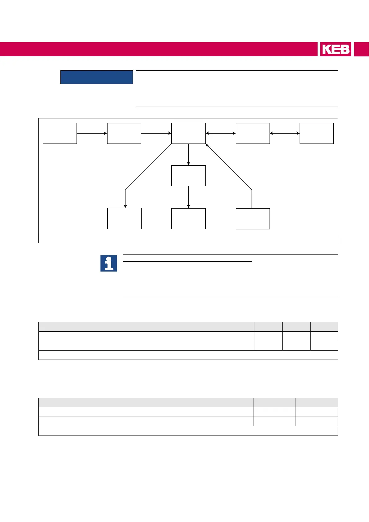
Net
Rectier
DC link
Inverter
Braking
transistor
Motor
DC Out
Braking
resistor
DC In
I
in IN
Iout_dc IB
Iin_dc
Figure 9: Block diagram of the energy ow
Activation of the braking transistor function
The function must be activated with parameter "is30 braking transistor func-
tion" in order to use the braking transistor.
Further information can be found in the download area of www.keb.de under
the search term „S6 Programming manual“.
3.6.5 Power dissipation 400 V devices
Device size 07 09 10
Power dissipation at rated operation
1)
PD / W 50 57 80
Power dissipation at DC supply
1)
PD_dc / W 31 46 63
Table 34: Power dissipation 400 V devices
1)
Rated operation corresponds to UN = 400 V; fSN; fout = 50 Hz (typically value).
3.6.6 Power dissipation 230 V devices
Device size 07 09
Power dissipation at rated operation
1)
PD / W 60 95
Power dissipation at DC supply
1)
PD_dc / W 70 50
Table 35: Power dissipation 230 V devices
1)
Rated operation corresponds to UN = 400 V; fSN; fout = 50 Hz (typically value).
49
GENERAL DATA
 Loading...