Radio Power Distribution: 2-1
Chapter 2 Radio Power Distribution
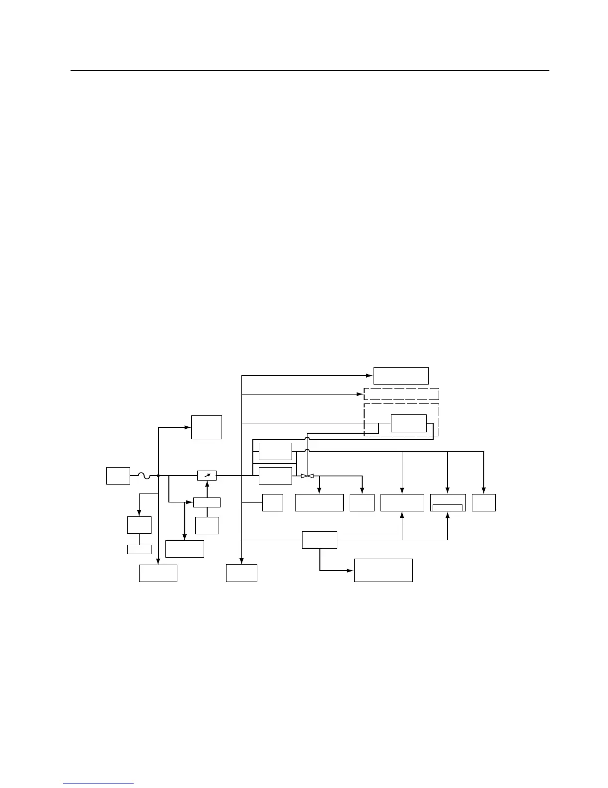
A block diagram of the DC power distribution throughout the radio board is shown in Figure 2-1. A
7.5V battery supplies the basic radio power (UNSWB) directly to the electronic on/off control, audio
power amplifier, 3.5V regulator, power amplifier automatic level control (ALC), and low battery detect
circuit. When the radio on/off/volume control is turned on, the switched SWB+ is applied to the
various radio power regulators, antenna switch, accessories 20-pin connector, keypad/option board,
and transmit LED. The Vdda signal from the 3.3V Vdda regulator supplies the microprocessor with
operating power. The Vdd regulator scheme is listed by band in Table 2-1 on page 2-2. Data is then
sent to the controller ASFIC to turn on a DAC which takes over the momentary-on path within 12ms.
The SWB+ signal supplies power until the radio is turned off. Jumpers for configuring the Vdda and
Vddd regulators are shown in Figure 2-1 and described in Table 2-2 on page 2-2.
The radio turns off when either of the two following conditions occur:
• Radio on/off/volume control is turned off.
• Low battery condition is detected.
If a low battery level is detected by the microprocessor through either of the above conditions, the
radio personality data is stored to EEPROM prior to turning off.
Figure 2-1. DC Power Distribution Block Diagram
SWB+
Fuse
Low Battery
Detect
Antenna
Switch
PA, Driver
PCIC(ALC)
LI Ion
3.5V
Reg.
Audio
Power
Amplifier
4.0V/3.3V
ASFIC_CMP
VCOBIC
FRACTN
LVZIF
LCD
Driver
5V
MECH.
SWB+
UNSWB+
Int/Ext Vdd
Vdda
Accessories
20 pin Connector
Keypad/Option Board
Prime Expansion Board
Switching
Regulator
Vdda
MCU, ROM
and EEPROM
Tx
Led
Control
7.5V
Battery
Vddd
Regulator
Vdda
Regulator
5V
Regulator
On/Off
Switch
RF, AMP, IF AMP
Ext. RX.
Buffer (NU)
 Loading...