7-14 Low Band, 800 MHz, PassPort & 900 MHz Theory of Operation: Synthesizer
7.8.1 Voltage Control Oscillator (VCO)
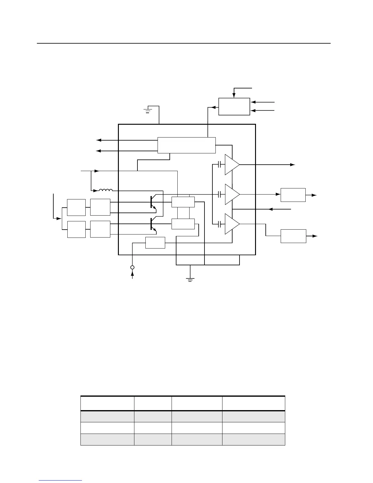
The voltage controlled oscillator block diagram is shown in Figure 7-10.
Figure 7-10. 800 MHz VCO Block Diagram
The VCOBIC (U250) in conjunction with the Low Voltage Fractional-N (LV FracN) synthesizer (U201)
generates RF in both the receive and the transmit modes of operation. The TRB line (U250 pin 19)
determines which oscillator and buffer will be enabled. A sample of the RF signal from the enabled
oscillator is routed from U250 pin 12, through a low pass filter, to the prescaler input (U201 pin 32).
After frequency comparison in the synthesizer, a resultant CONTROL VOLTAGE is received at the
VCO. This voltage is a DC voltage between 2.0 V (low frequency) and 11.0 V (high frequency) when
the PLL is locked on frequency.
The VCOBIC (U250) is operated at 4.54 V (VSF) and LV FracN synthesizer (U201) at 3.3 V. This
difference in operating voltage requires a level shifter consisting of Q200 and Q252 on the TRB line.
The operation logic is shown in Tab l e 7 - 1 .
Table 7-1. Level Shifter Logic
Desired Mode AUX 4 AUX 3 TRB
Tx Low High (@3.2V) High (@4.8V)
Rx High Low Low
Battery Saver Low Low Hi-Z/Float (@2.5V)
Presc
RX
TX
Injection
Amplifier
Buffer
Amplifier
Pin 8
Pin 14
Pin 10
5V
(U201 Pin 28
VCC Buffers
TX RF Injection
U201 Pin 3
AUX4 (U201 Pin 3)
AUX3 (U201 Pin 2)
Prescaler Out
Pin 12
Pin 19
Pin 20
TX/RX/BS
Switching Network
U250
VCOBIC
Rx Active
Bias
Tx Active
Bias
Pin 2
Rx-I adjust
Pin 1
Tx-I adjust
Pins 9,11,17
Pin 18
Vsens
Circuit
Pin 15
Pin 16
TX VCO
Circuit
TX
Tank
RX VCO
Circuit
RX
Tank
Pin 7
Vcc-Superfilter
Collector/RF in
Pin 4
Pin 5
Pin 6
RX
TX
(U201 Pin 28)
Rx-SW
Tx-SW
Vcc-Logic
(U201 Pin 28)
teer Line
Voltage
(VCTRL)
Pin 13
Pin 3
TRB_IN
LO RF INJECTION
Level Shifter
Network
VSF
VSF
VSF
 Loading...