Low Band, 800 MHz, PassPort & 900 MHz Theory of Operation: Synthesizer 7-5
The synthesizer is powered by regulated 5V and 3.3 V. The 5 volt signal to the synthesizer as well as
the rest of the radio is provided by U204. The 3.3 V signal is provided by U200 in the controller. The
5V signal goes to pins 13 and 30 while the 3.3 V signal goes to pins 5, 20, 34 and 36 of U201. The
synthesizer in turn generates a superfiltered 4.3 V which powers the VCOs and buffers.
In addition to the VCO, the synthesizer also interfaces with the logic and ASFIC circuitry.
Programming for the synthesizer is accomplished through the data, clock and chip select lines (pins
7, 8 and 9) from the microprocessor, U409. A 3.3 V dc signal from pin 4 indicates to the
microprocessor that the synthesizer is locked.
Transmit modulation from the ASFIC is supplied to pin10 of U205. Internally the audio is digitized by
the LV FracN IC and applied to the loop divider to provide the low-port modulation. The audio runs
through an internal attenuator for modulation balancing purposes before going out at pin 41 to the
VCO.
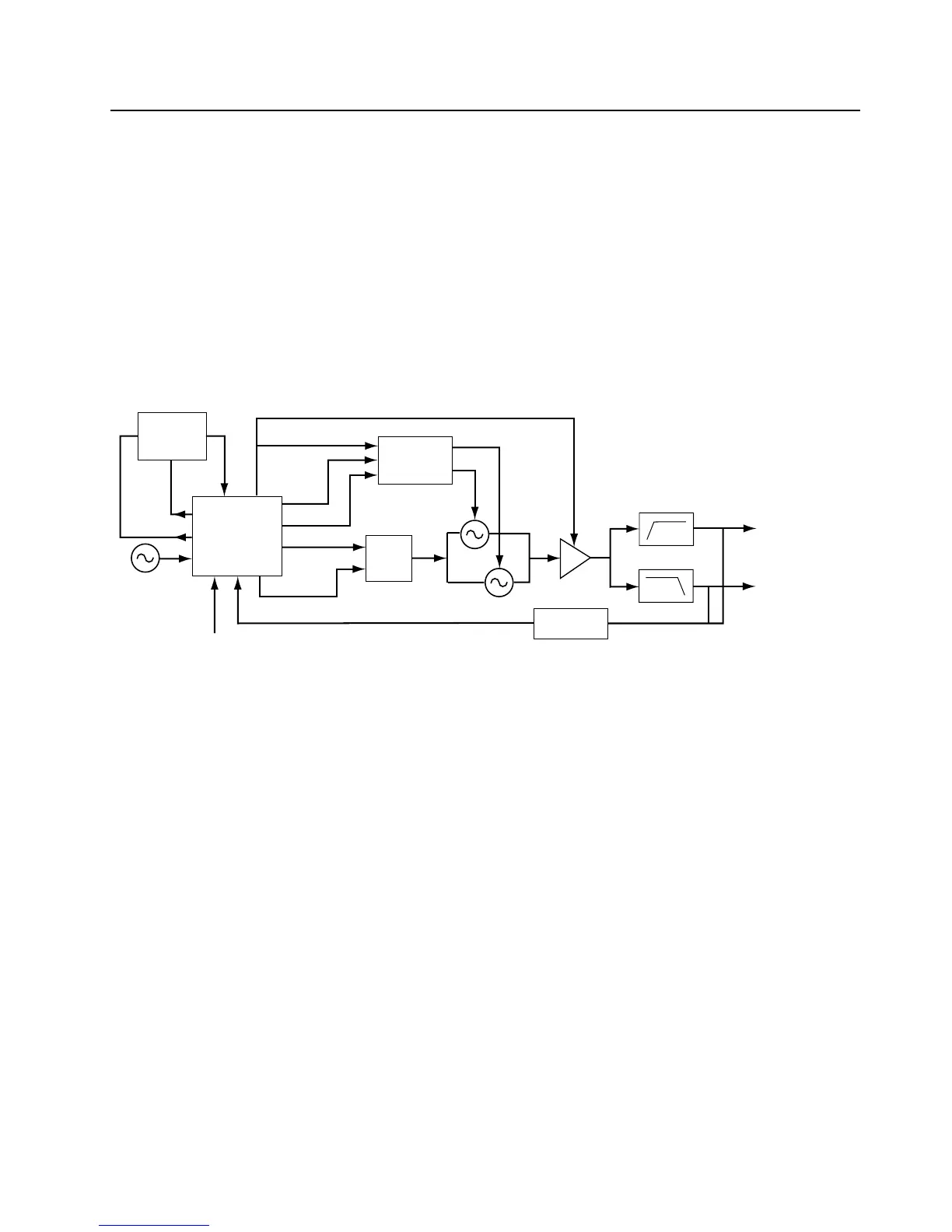
Figure 7-3. Low Band Frequency Generation Unit Block Diagram
7.4 Synthesizer
The Low Voltage Fractional-N (LV FracN) synthesizer, shown in Figure 7-4 on page 7-6, uses a 17.0
MHz crystal (Y201) to provide a reference for the system. Along with being used in the LV FracN
synthesizer, the 17.0 MHz signal is provided at pin 19 of U205 for use by the ASFIC and LVZIF.
The LV FracN IC (U205) further divides this by 8 internally to give 2.125 MHz to be used as the
reference frequency in the frequency synthesis. While UHF and VHF can use other references,
(divide by 7 or divide by 7/8), only the divide by 8 function is valid for lowband.
The internal oscillator device in the LV FracN IC together with C236, C237, C242, R219, CR211and
Y201 comprise the reference oscillator. This oscillator is temperature compensated is capable of 2.5
ppm stability over temperatures of -30° to 85°C. There is temperature compensation information that
is unique to each crystal contained on Y201 that is programmed into the radio when built.
The loop filter consists of components C256, C257, C259, R224, R225 and R228. This circuit
provides the necessary dc steering voltage for the VCO and determines the amount of noise and
spur passing through.
To achieve fast locking for the synthesizer, an internal adapt charge pump provides higher current at
pin 45 of U205 to put the synthesizer within lock range. The required frequency is then locked by
normal mode charge pump at pin 43.
Synthesizer
U205
Voltage
Multiplier
Switching
Network
Loop
Filter
To Mixer
To PA Driv
VCP
VSF
Vmult2
Vmult1
Aux2
Prescaler Input
Modulating
Signal
Rx VCO
Circuit
Tx VCO
Circuit
7.0 MHz
ef. Osc.
Buffer
Amplifier
Aux3
MOD Out
 Loading...