UHF Band 2 Theory of Operation: Synthesizer 5-5
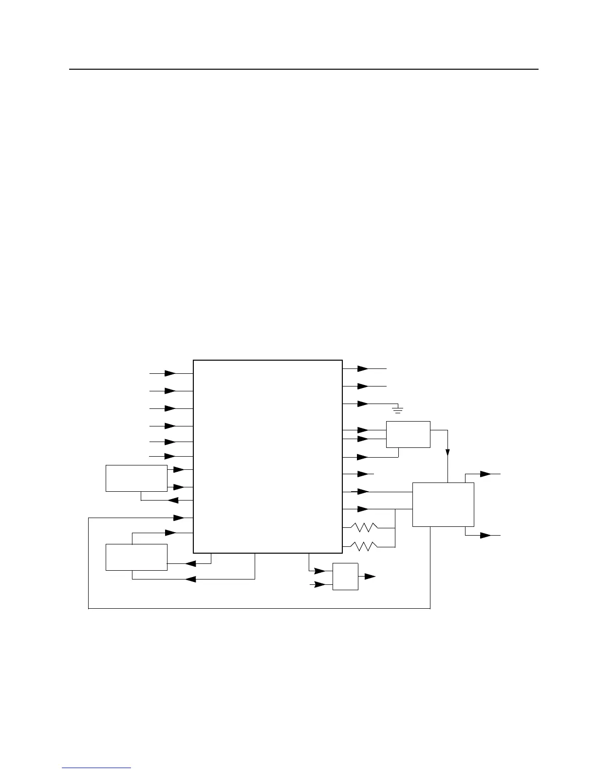
The Frequency Generation Circuitry is composed of two main ICs:
• Fractional-N synthesizer (U201)
• VCO/Buffer IC (U241)
Designed in conjunction to maximize compatibility, the two ICs provide many of the functions that
normally would require additional circuitry. The synthesizer block diagram illustrates the interconnect
and support circuitry used in the region. Refer to the relevant schematics for the reference
designators.
The synthesizer is powered by regulated 5 V and 3.3 V, which come from U247 and U248,
respectively. The synthesizer in turn generates a superfiltered 4.5 V which powers U241.
In addition to the VCO, the synthesizer must interface with the logic and ASFIC circuitry.
Programming for the synthesizer is accomplished through the data, clock and chip select lines from
the microprocessor. A 3.3 V DC signal from synthesizer lock detect line indicates to the
microprocessor that the synthesizer is locked.
Transmit modulation from the ASFIC is supplied to pin 10 of U201. Internally, the audio is digitized by
the Fractional-N and applied to the loop divider to provide the low-port modulation. The audio runs
through an internal attenuator for modulation balancing purposes before going out to the VCO.
5.4 Synthesizer
(Refer to the UHF Synthesizer Schematic Diagram on page 9-220.)
Figure 5-4. Synthesizer Block Diagram
The Fractional-N Synthesizer uses a 16.8 MHz crystal (FL201) to provide a reference for the system.
The LVFractN IC (U201) further divides this to 2.1 MHz, 2.225 MHz, and 2.4 MHz as reference
frequencies. Together with C206, C207, C208, R204, and CR203, they build up the reference
oscillator which is capable of 2.5 ppm stability over temperatures of –30 to 85°C. It also provides
16.8 MHz at pin 19 of U201 to be used by ASFIC.
DATA
CLK
CEX
MODIN
VCC, DC5V
XTAL1
XTAL2
WARP
PREIN
VCP
REFERENCE
OSCILLATOR
VOLTAGE
MULTIPLIER
VOLTAGE
CONTROLLED
OSCILLATOR
2-POLE
LOOP
FILTER
DATA (U409 PIN 100)
CLOCK (U409 PIN 1)
CSX (U409 PIN 2)
MOD IN (U404 PIN 40)
+5V (U247 PIN 4)
7
8
9
10
13, 30
23
24
25
32
47
VMULT2 VMULT1
BIAS1
SFOUT
AUX3
AUX4
IADAPT
IOUT
GND
FREFOUT
LOCK
4
19
6, 22, 23, 24
43
45
3
2
28
14
15
40
FILTERED 5V
STEERING
LINE
LOCK (U409 PIN 56)
PRESCALER IN
LO RF INJECTION
TX RF INJECTION
(1ST STAGE OF PA
FREF (U201 PIN 21 & U404 PIN 34)
39
BIAS2
41
DUAL
TSTRS
48
5V
R5
5, 20, 34, 36
(U248 PIN 5)
AUX1
VDD, 3.3V
MODOUT
U251
LOW VOLTAGE
FRACTIONAL-N
SYNTHESIZER
 Loading...