Low Band, 800 MHz, PassPort & 900 MHz Theory of Operation: 900 MHz Receiver 7-19
U103 and its associated components are part of the temperature cut back circuitry. It senses the
printed circuit board temperature around the transmitter circuits and output a DC voltage to the
PCIC. If the DC voltage produced exceeds the set threshold in the PCIC, the transmitter output
power will be reduced so as to reduce the transmitter temperature.
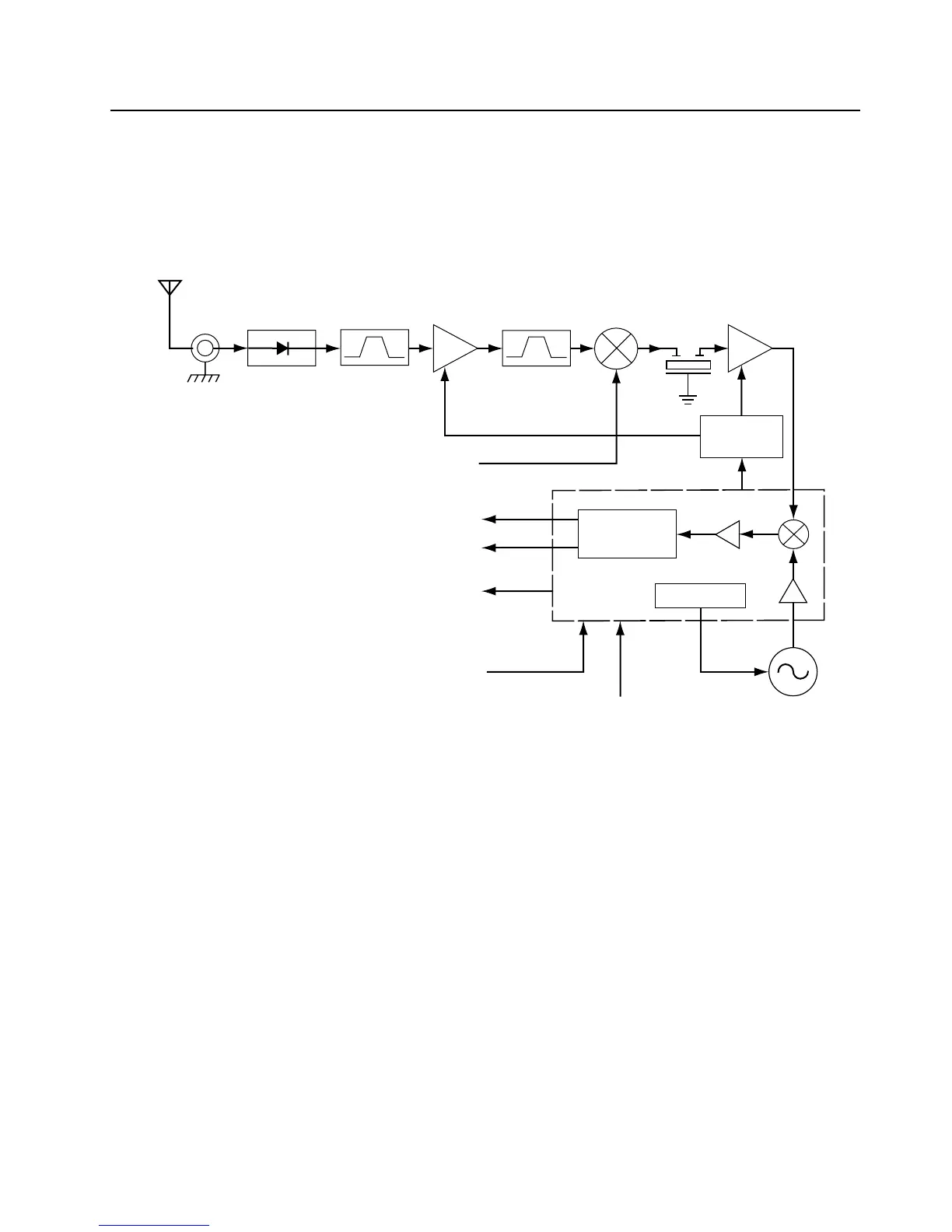
7.11 900 MHz Receiver
Figure 7-12. 900 MHz Receiver Block Diagram (for PCB No. 8485910Z01)
Demodulator
Synthesizer
Crystal
Filter
Mixer
RF
Amp
IF
Amp
3-Pole
Ceramic
Block Filter
3-Pole
Ceramic
Block Filter
ntenna
First LO
from FGU
Recovered Audio
Squelch
RSSI
IF
IC
SPI Bus
16.8 MHz
Reference Clock
Secon
LO VC
RFJack
Pin Diode
Antenna
Switch
AGC
Processing
U351
 Loading...