7-26 Low Band, 800 MHz, PassPort & 900 MHz Theory of Operation: 900 MHz Voltage Control Oscillator (VCO)
7.14 900 MHz Voltage Control Oscillator (VCO)
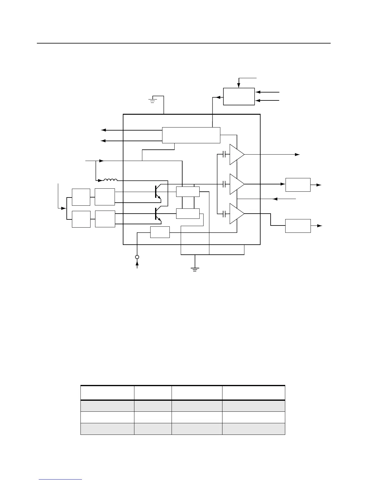
Figure 7-16. VCO Block Diagram
The VCOBIC (U250) in conjunction with the LV FracN synthesizer (U201) generates RF in both the
receive and the transmit modes of operation. The TRB line (U250 pin 19) determines which oscillator
and buffer will be enabled. A sample of the RF signal from the enabled oscillator is routed from U250
pin 12, through a low pass filter, to the prescaler input (U201 pin 32). After frequency comparison in
the synthesizer, a resultant CONTROL VOLTAGE is received at the VCO. This voltage is a DC
voltage between 2.0 V (low frequency) and 11.0 V (high frequency) when the PLL is locked on
frequency.
The VCOBIC (U250) is operated at 4.54 V (VSF) and LV FracN synthesizer (U201) at 3.3 V. This
difference in operating voltage requires a level shifter consisting of Q200 and Q252 on the TRB line.
The operation logic is shown in Tab l e 7 - 3 .
Table 7-3. Level Shifter Logic
Desired Mode AUX 4 AUX 3 TRB
Tx Low High (@3.2V) High (@4.8V)
Rx High Low Low
Battery Saver Low Low Hi-Z/Float (@2.5V)
Presc
RX
TX
Injection
Amplifier
Buffer
Amplifier
Pin 8
Pin 14
Pin 10
5V
(U201 Pin 28
VCC Buffers
TX RF Injection
U201 Pin 3
AUX4 (U201 Pin 3)
AUX3 (U201 Pin 2)
Prescaler Out
Pin 12
Pin 19
Pin 20
TX/RX/BS
Switching Network
U250
VCOBIC
Rx Active
Bias
Tx Active
Bias
Pin 2
Rx-I adjust
Pin 1
Tx-I adjust
Pins 9,11,17
Pin 18
Vsens
Circuit
Pin 15
Pin 16
TX VCO
Circuit
TX
Tank
RX VCO
Circuit
RX
Tank
Pin 7
Vcc-Superfilter
Collector/RF in
Pin 4
Pin 5
Pin 6
RX
TX
(U201 Pin 28)
Rx-SW
Tx-SW
Vcc-Logic
(U201 Pin 28)
teer Line
Voltage
(VCTRL)
Pin 13
Pin 3
TRB_IN
LO RF INJECTION
Level Shifter
Network
VSF
VSF
VSF
 Loading...