Power
PRELIMINARY INFORMATION
Jetson Orin NX Series and Jetson Orin Nano Series DG-10931-001_v1.1 | 23
6.1.1.1 Defined Behaviors
For all actions triggered by SLEEP/WAKE* or ACOK, there will be a de-bounce time before
triggering any output signal. The minimum I/O delay for these signals is therefore the de-
bounce time. De-bounce time is 20 ms. If both signals above are triggered within the 20 ms
de-bounce time started by the first detected signal, then the de-bounce time for the
subsequent signals might extend up to 25 ms.
Note: The time values in the following timing diagrams have an accuracy of ± 10%.
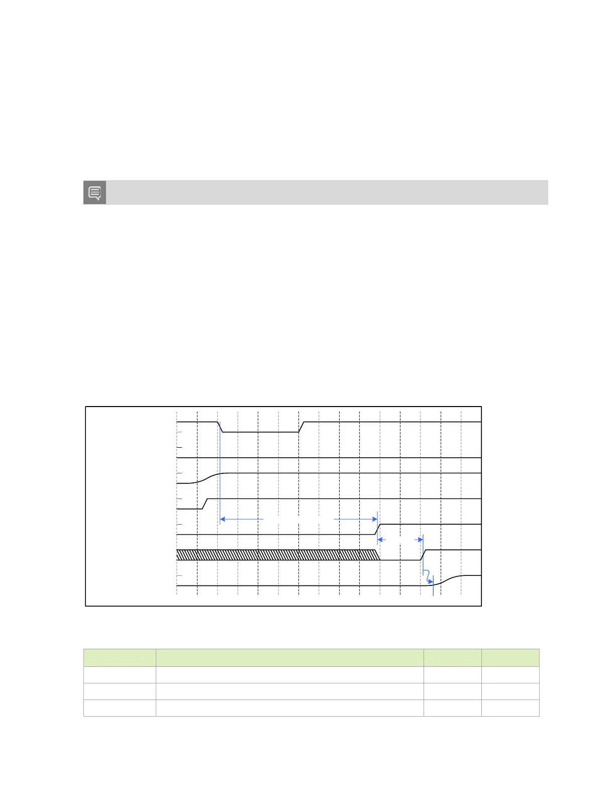
6.1.1.2 Power-Off -> Power-On (Power Button Case)
Power button press use case: User presses the Power Button briefly, and the MCU sends the
power enable signal to the module (POWER_EN) and on to the Power Sequencer on the Orin
module. The signal representing the Power Button to the Orin Module (SLEEP/WAKE* pin), will
have the same (brief) duration of the Power Button input to the MCU. Once the power button is
pressed, the power OK input (ACOK) is ignored, as the power-on sequence is already initiated
by the power button.
If power-on is successful, SHUTDOWN_REQ* goes high.
Figure 6-8. Power-Off to On Sequence Power Button Case
POWER_EN
SLEEP/WAKE*
SYS_RESET*
ACOK
VDD_DCIN
SHUTDOWN_REQ*
T_PE_RST
Carrier Board 1.8V/
3.3V Supplies
T_PB_DET + T_VPWR_ON
Table 6-3. Power-Off to On Timing Power Button Case
SLEEP/WAKE* (power button) detect (de-bounce only)
Delay from power button active to POWER_EN
SYS_RESET* inactive delay from POWER_EN rising edge
 Loading...


