Miscellaneous Interfaces
PRELIMINARY INFORMATION
Jetson Orin NX Series and Jetson Orin Nano Series DG-10931-001_v1.1 | 71
Max trace length/delay (Branch-A) for MOSI, MISO, SCK and CS
2x-load star/daisy
Max trace length/delay skew from MOSI, MISO and CS to SCK
Note: Up to four signal vias can share a single GND return via
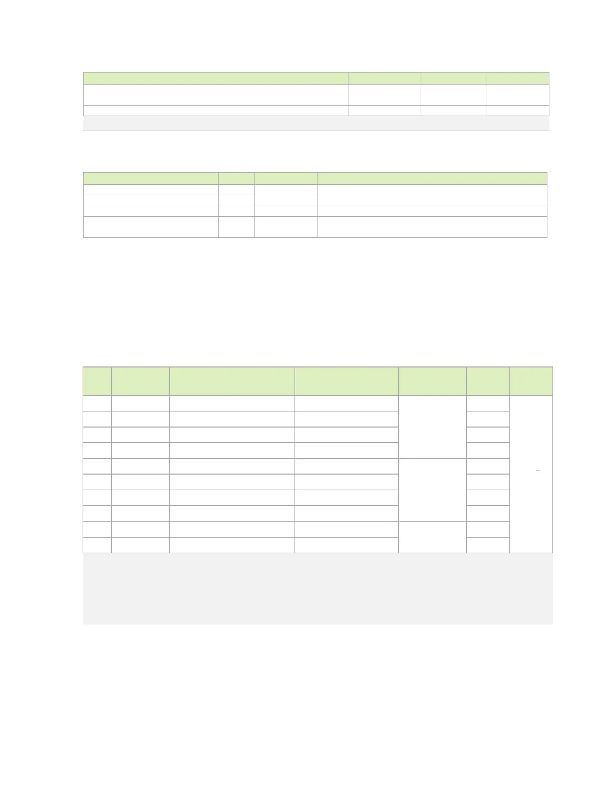
Table 12-6. SPI Signal Connections
Module Pin Names (Function)
SPI Clock.: Connect to peripheral CLK pins
SPI Data Output: Connect to target peripheral MOSI pins
SPI Data Input: Connect to target peripheral MISO pins
SPI Chip Selects.: Connect one CSx* pin per SPI interface to
each target peripheral CS pin on the interface
12.3 UART
The Orin module brings three UARTs out to the main connector. See Figure 12-5 for typical
assignments of the three available UARTs.
Table 12-7. Orin Module UART Pin Descriptions
UART general
(i.e. M.2 Key E)
GP70_UART1_TX_BOOT2_STRAP
Notes:
1. In the Direction column, Output is from Orin module. Input is to Orin module. Bidir is for Bidirectional signals.
2. The direction indicated for the UART pins except for is true when used for that function. Otherwise, these pins support GPIO
functionality and most can support both input and output (bidirectional) functionality. The exception is UART0_TXD, UART0_RTS*
and UART1_TXD. These have output-only buffers on the module to keep them from being affected by connected devices during
boot as they are associated with SoC strapping pins.
 Loading...


