USB and PCIe
PRELIMINARY INFORMATION
Jetson Orin NX Series and Jetson Orin Nano Series DG-10931-001_v1.1 | 27
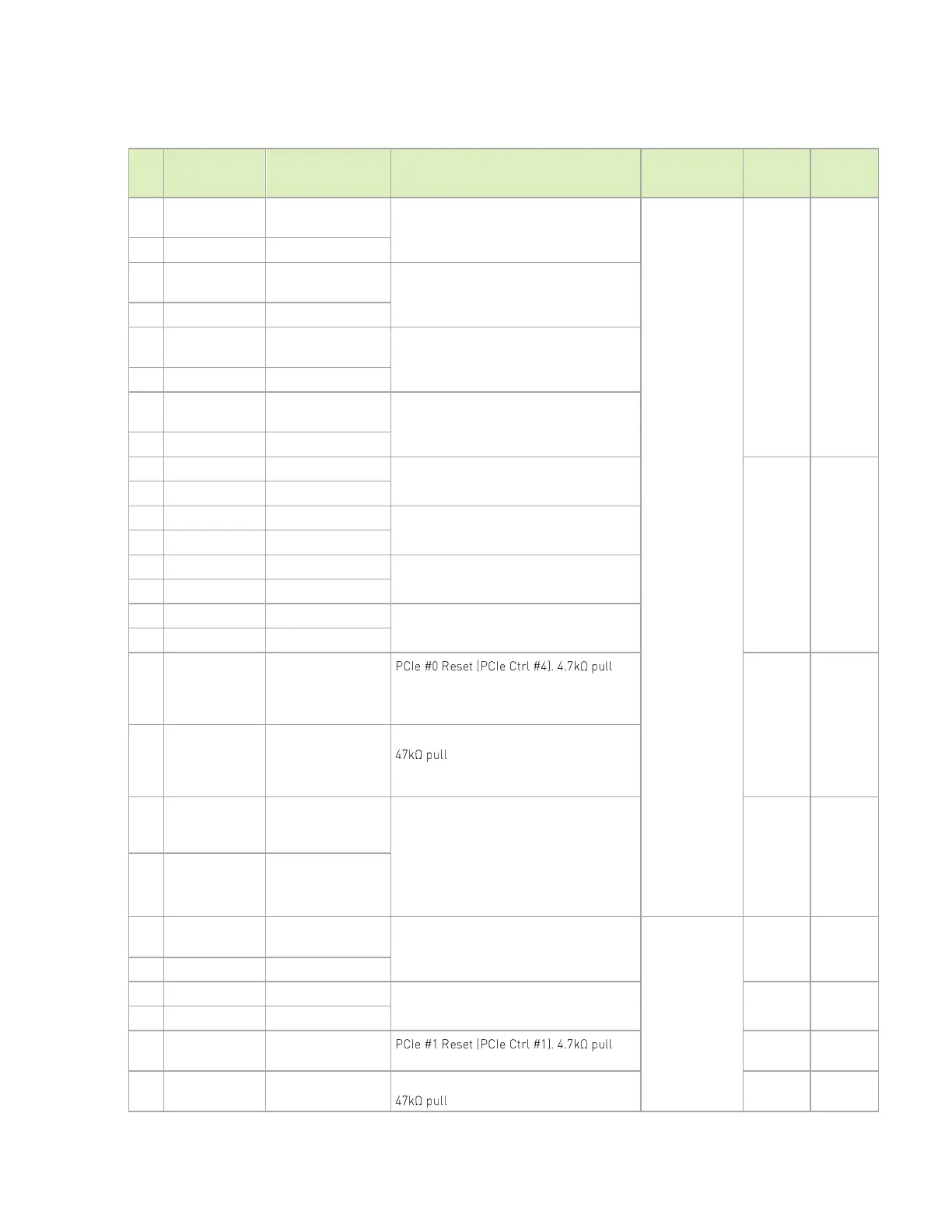
Table 7-2. Jetson Orin Module USB 3.2 and PCIe Pin Description
Orin SoC Pin Name
(See Note 4)
PCIe #0 Receive 0 (PCIe Ctrl #4 Lane 0)
PCIe x4
conn/device (i.e.
M.2 Key M)
PCIe #0 Receive 1 (PCIe Ctrl #4 Lane 1)
PCIe #0 Receive 2 (PCIe Ctrl #4 Lane 2)
PCIe #0 Receive 3 (PCIe Ctrl #4 Lane 3)
PCIe #0 Transmit 0 (PCIe Ctrl #4 Lane 0)
PCIe #0 Transmit 1 PCIe Ctrl #4 Lane 1)
PCIe #0 Transmit 2 (PCIe Ctrl #4 Lane 2)
PCIe #0 Transmit 3 (PCIe Ctrl #4 Lane 3)
-up
to 3.3V on the module. Output when module
is Root Port or input when module is
Endpoint.
PCIE #0 Clock Request (PCIe Ctrl #4).
-up to 3.3V on the Orin module.
Input when Orin module is Root Port or
output when Orin module is Endpoint.
SF_PCIE4_CLK_N
HS_UPHY0_
REFCLK2_N
PCIe #0 Reference Clock controlled by on-
module mux by SoC GP21. When GP21 is
low, SF_PCIE4_CLK is selected (reference
clock when Orin module is Root Port). When
GP21 is high, UPHY0_REFCLK2_IN is
selected (reference clock input when Orin
module is an Endpoint).
SF_PCIE4_CLK_P
HS_UPHY0_
REFCLK2_P
PCIe #1 Receive 0 (PCIe Ctrl #1 Lane 0)
PCIe x1
conn/device (i.e.
M.2 Key E)
PCIe #1 Transmit 0 (PCIe Ctrl #1 Lane 0)
-up
to 3.3V on the module.
PCIE #1 Clock Request (PCIe Ctrl #1).
-up to 3.3V on the module.
 Loading...


