Miscellaneous Interfaces
PRELIMINARY INFORMATION
Jetson Orin NX Series and Jetson Orin Nano Series DG-10931-001_v1.1 | 70
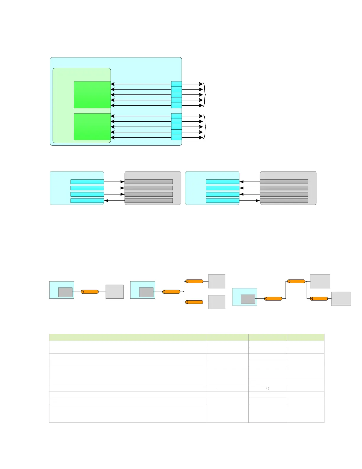
Figure 12-2. SPI Connections
Jetson
SoC SPI
SPI0_SCK
SPI0_MISO
SPI0_MOSI
SPI0_CS0*
SPI0_CS1*
SPI1_SCK
SPI_MISO
SPI1_MOSI
SPI1_CS0*
SPI1_CS1*
GP47_SPI1_SCK
GP48_SPI1_MISO
GP49_SPI1_MOSI
GP50_SPI1_CS0
GP51_SPI1_CS1
Connect to up to 2 SPI
devices (separate CS
for each)
91
89
93
95
97
GP36_SPI3_SCK
GP37_SPI3_MISO
GP38_SPI3_MOSI
GP39_SPI3_CS0
GP40_SPI3_CS1
106
104
108
110
112
Connect to up to 2 SPI
devices (separate CS
for each)
Figure 12-3. Basic SPI Initiator and Target Connections
Jetson Initiator
SPIn_CSx
SPIn_SCK
SPIn_MOSI
SPIn_MISO
SPI Target
CS (Chip Select)
CLK (Clock)
MOSI (Master out, Slave in)
MISO (Master in, Slave out)
Jetson Target
SPIn_CSx
SPIn_SCK
SPIn_MOSI
SPIn_MISO
SPI Initiator
CS (Chip Select)
CLK (Clock)
MOSI (Master out, Slave in)
MISO (Master in, Slave out)
12.2.1 SPI Routing Guidelines
The following guidelines meet the SPI routing guidelines.
Figure 12-4. SPI Topologies
Jetson
SPI
Device
#1
Main trunk
SPI
Device
#2
SPI
Device
#1
Main trunk
SPI
Device
#2
Branch-A
Branch-B
Branch-A
Branch-B
2x-Load Star Topology 2x-Load Daisy Topology
SPI
Device
Main trunk
SoC
Jetson
SoC
Jetson
SoC
Point-Point Topology
Table 12-5. SPI Interface Signal Routing Requirements
Configuration / device organization
Max loading (total of all loads)
Breakout region impedance
Minimum width
and spacing
Via proximity (signal to reference)
Trace spacing: Microstrip / Stripline
Max trace length/delay (PCB main trunk) For MOSI, MISO, SCK and CS
Point-point
2x-load star/daisy