Display
PRELIMINARY INFORMATION
Jetson Orin NX Series and Jetson Orin Nano Series DG-10931-001_v1.1 | 53
9.2.1 HDMI Routing Guidelines
This section describes the HDMI routing guidelines for the Orin module.
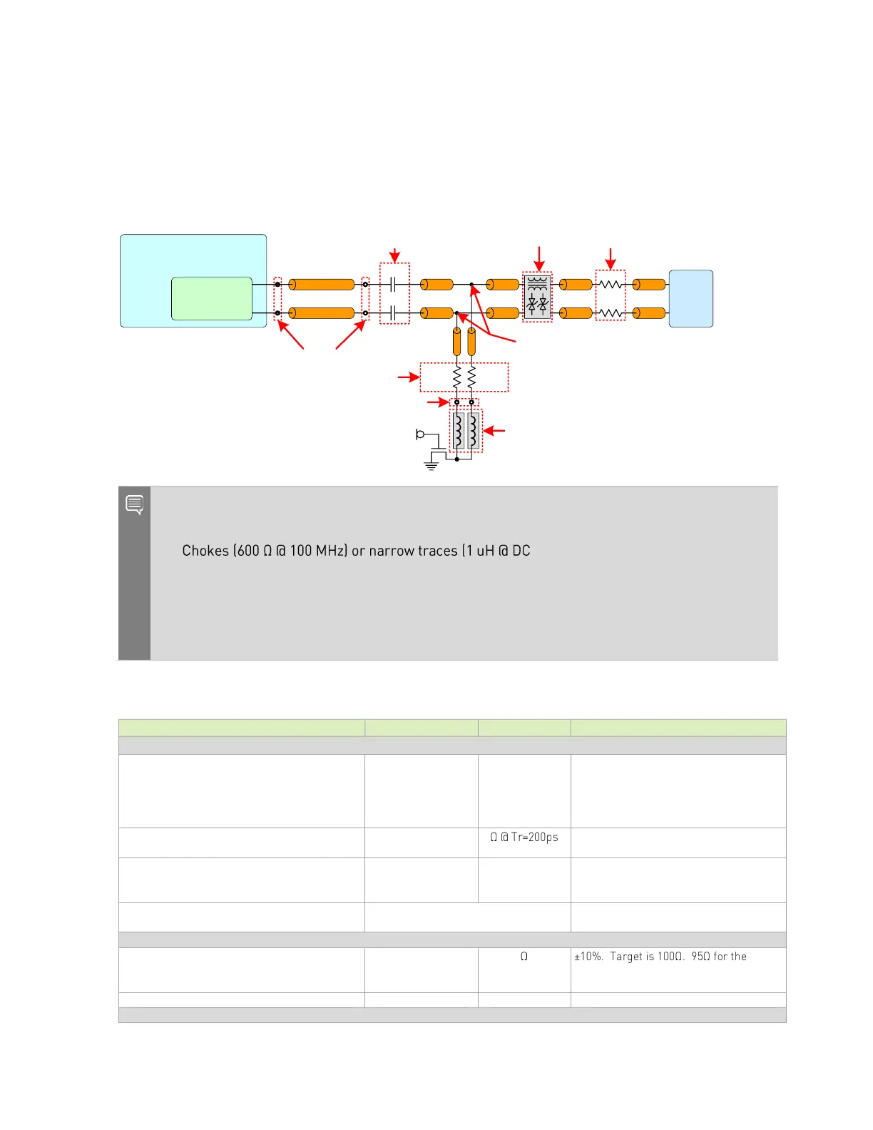
Figure 9-7. HDMI CLK and Data Topology
Jetson
HDMI
Conn
AC
CAP
Seg D Seg F
MOD_SLEEP*
499Ω,
1%
PCB Vias
PCB Vias
0.1uF
0.1uF
R
PD
Common Mode
Chokes & ESD
See Note 1
499Ω,
1%
Seg B Seg E
Seg C
SoC
-
-
Main Route –
Seg A
* Note 3 * Note 3* Note 3 * Note 3
R
S
(See Note 4)
Choke or Trace
See Note 2
Notes:
1. RPD pad must be on the main trace. RPD and ACCAP must be on same layer.
2. -100 MHz) between pull-downs and
FET are chokes between pull-downs and FET are optional improvements for HDMI 2.0
operation.
3. The trace after the main route via should be routed on the top or bottom layer of the PCB,
and either with 100 ohm differential impedance, or as uncoupled 50 ohm SE traces.
4. See the RS section in Table 9-5 for details.
Table 9-5. HDMI Interface Signal Routing Requirements
IL
Resonance dip frequency
<= 1.7
<= 2
<= 3
< 4.3
> 12
dB @ 1GHz
dB @ 1.5GHz
dB @ 3GHz
dB @ 6GHz
GHz
For HDMI 2.0, 6 dB and 6 GHz is
supported.
10%-90%. If TDR dip is 75~85 ohm that
dip width should < 250 ps
dB at DC
dB at 3GHz
dB at 6GHz
IL/FEXT plot: See HDMI Guideline
Figure 9-8
Trace impedance: Diff pair
breakout and main route is an
implementation option.
Trace spacing/Length/Skew
 Loading...


