USB and PCIe
PRELIMINARY INFORMATION
Jetson Orin NX Series and Jetson Orin Nano Series DG-10931-001_v1.1 | 38
4. Isolation circuitry is required on the PCIe control signals when Orin module is configured as
Endpoint. These isolate the lines from the on-module pull-ups as well as ensure the
Endpoint and Root Port devices do not have their pads driven high before power is applied.
5. The PCIe REFCLK inputs and PCIEx_CLK clock outputs comply to the PCIe CEM specification
7.2.1 PCIe Routing Guidelines
The following table provides the PCIe routing guidelines for Gen3 and Gen4.
Table 7-10. PCIe Interface Signal Routing Requirements up to Gen4
Data Rate / UI Period
Gen3
Gen4
Unidirectional, differential. Driven by
100MHz common reference clock
To GND Single Ended for P and N
Trace Impedance
differential / Single Ended
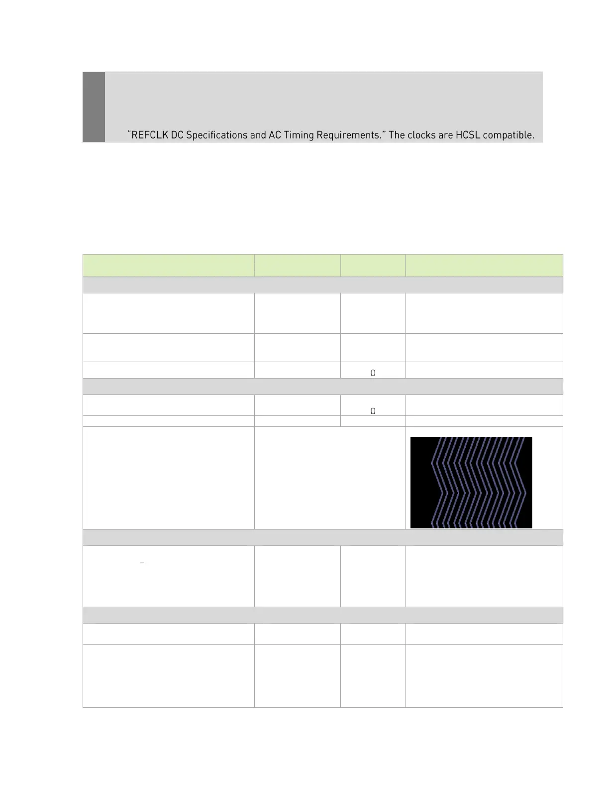
Fiber-weave effect (Only required for Gen4)
• Use spread-glass (denser weave)
instead of regular-glass (sparse
weave) to minimize intra-pair skew
• Use zig-zag route instead of straight
to minimize skew, this is mandatory
for PCIe gen4 design
Example of zig-zag routing.
Trace Spacing (Stripline)
Pair Pair
To plane and capacitor pad
To unrelated high-speed signals
TX and RX should not be routed on the
same layer. If this is required in a design,
they should not be interleaved, and the
spacing between the closest RX and TX
lanes must be 9x Dielectric height
spacing.
Breakout region (Max delay)
Minimum width and spacing. 4x or wider
dielectric height spacing is preferred
Gen 4.0 max trace loss / length (delay):
Direct to device:
Insertion loss / length (delay)
Routing to 2
nd
Orin Module
Insertion loss / length (delay)
-20.51 / 345 (2208)
-14.74 / 248 (1587)
Direct to device Insertion loss budget is
for PCB routing, connectors, and end
device (See Note 1). EM-370(Z) PCB
material is assumed in the length/delay
calculations:
 Loading...


