MIPI CSI Video Input
PRELIMINARY INFORMATION
Jetson Orin NX Series and Jetson Orin Nano Series DG-10931-001_v1.1 | 60
Table 10-2. Orin Module Camera Miscellaneous Pin Descriptions
Camera I2C. 2.2 -up to 3.3V on the
module.
Camera 0 Powerdown or GPIO
Camera 1 Powerdown or GPIO
GPIO #1 or Generic Clock Output #1
GPIO #11 or Generic Clock Output #2
Notes:
1. In the Direction column, Output is from Orin module. Input is to Orin module. Bidir is for Bidirectional signals.
2. The direction shown in this table for CAM[1:0]_MCLK and CAM[1:0]_PWDN is true when used for those functions. These pins are
GPIOs and can support input or output (bidirectional). The direction indicated for GPIO01 and GPIO11 is associated with their use
as clock outputs.
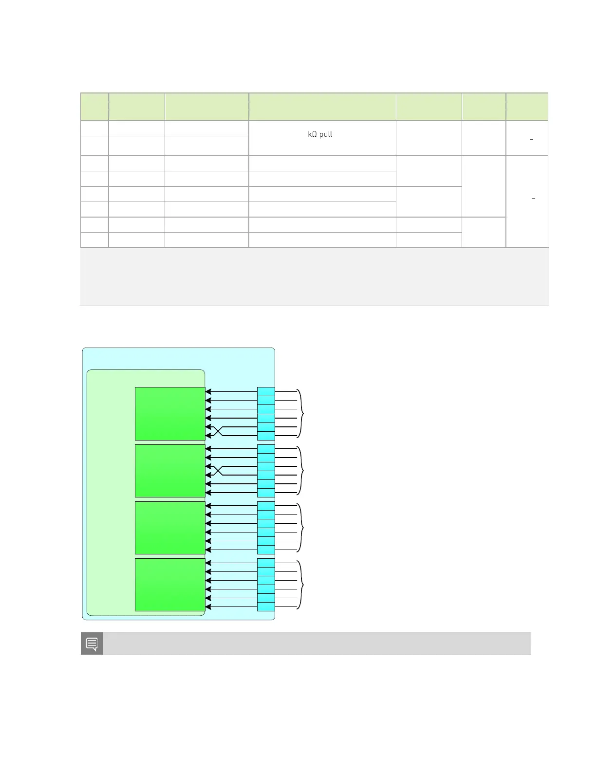
Figure 10-1. CSI 2-Lane Connection Options
Jetson
SoC
HS_CSI0_CLK_N
HS_CSI0_CLK_P
HS_CSI0_D0_N
HS_CSI0_D0_P
HS_CSI0_D1_N
HS_CSI0_D1_P
Camera 1
(2-Lane)
HS_CSI1_CLK_N
HS_CSI1_CLK_P
HS_CSI1_D0_N
HS_CSI1_D0_P
HS_CSI1_D1_N
HS_CSI1_D1_P
CSI_0_CLK_N
CSI_0_CLK_P
CSI_0_D0_N
CSI_0_D0_P
CSI_0_D1_N
CSI_0_D1_P
CSI1_CLK_N
CSI1_CLK_P
CSI1_D0_N
CSI1_D0_P
CSI1_D1_N
CSI1_D1_P
CSI2_CLK_N
CSI2_CLK_P
CSI2_D0_N
CSI2_D0_P
CSI2_D1_N
CSI2_D1_P
CSI3_CLK_N
CSI3_CLK_P
CSI3_D0_N
CSI3_D0_P
CSI3_D1_N
CSI3_D1_P
Camera 3
(2-Lane)
10
HS_CSI3_CLK_N
HS_CSI3_CLK_P
HS_CSI3_D0_N
HS_CSI3_D0_P
HS_CSI3_D1_N
HS_CSI3_D1_P
HS_CSI2_CLK_N
HS_CSI2_CLK_P
HS_CSI2_D0_N
HS_CSI2_D0_P
HS_CSI2_D1_N
HS_CSI2_D1_P
Camera 4
(2-Lane)
12
4
6
16
18
3
5
15
17
28
30
22
24
34
36
27
29
21
23
33
35
9
11
Camera 2
(2-Lane)
Note: CSI_0_D1 and CSI_1_D0 have P/N swapped on the module.
 Loading...


