USB and PCIe
PRELIMINARY INFORMATION
Jetson Orin NX Series and Jetson Orin Nano Series DG-10931-001_v1.1 | 33
signal vias (2 diff pairs) can share a
single GND return via
Max # of Vias
PTH vias
Micro Vias
4 if all vias are PTH via
Not limited if total channel loss meets IL spec
long via stub requires review (IL and
resonance dip check)
Dimension
Min A Spacing
Min B, C Length
Min Jog Width
S1 must be taken care
in order to consider
Xtalk to adjacent pair.
Additional Component Placement Order
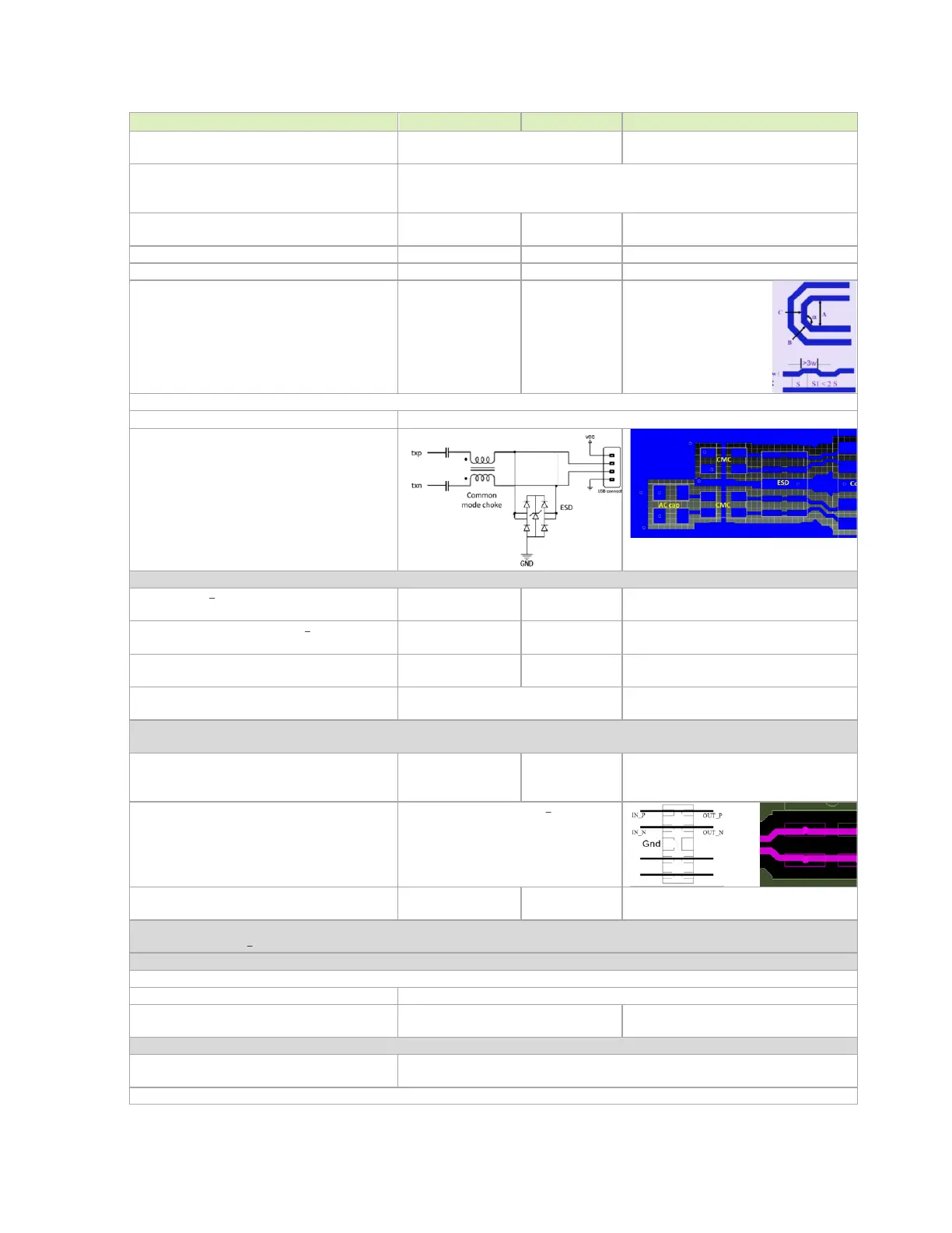
Chip AC capacitor (TX only) common mode choke ESD Connector
100nF recommended. Only required for
TX pair when routed to connector.
Value on RX (connector case) Min/Max
Optional. 330 nF recommended if
placed.
Location (max length to adjacent
discontinuity)
Discontinuity is connector, via, or
component pad
GND/PWR void under/above cap is
preferred
Voiding is required if AC cap size is 0603
or larger
ESD (On-chip protection diode can withstand 2kV HMM. External ESD is optional. Designs should include ESD footprint as a
stuffing option)
Max Junction capacitance (IO to GND)
Gen1
Gen2
Gen1: SEMTECH RClamp0524p
Gen2: TPD4E02B04DQA
Pad should be on the net not trace
stub
Location (max length to adjacent
discontinuity)
Discontinuity is connector, via, or
component pad
Common-mode Choke
(Not recommended only used if absolutely required for EMI issues). See Chapter 17 for details on CMC if implemented.
FPC (Additional length of Flexible Printed Circuit Board)
The FPC routing should be included for PCB trace calculations (max length, etc.)
Strongly recommend being the same
as the PCB or better
If worse than PCB, the PCB and FPC
length must be re-estimated
SMT Connector GND Voiding
GND plane under signal pad should be voided. Size of void should be the same
size as the pad.
Connector used must be USB-IF certified
 Loading...


