LTE-A Module Series
EG060V-EA Hardware Design
EG060V-EA_Hardware_Design 32 / 82
3.6.2. Decrease Voltage Drop
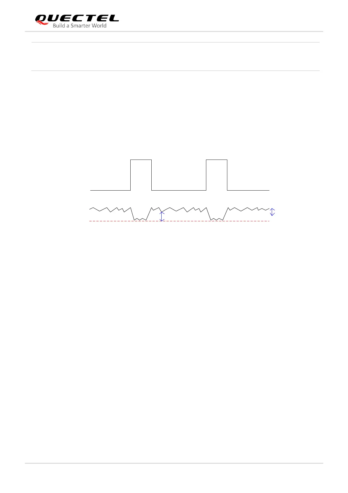
The power supply range of the module is from 3.3 to 4.3 V. Please make sure the input voltage never
drops below 3.3 V. The following figure shows the voltage drop in case of burst transmission in 3G and
4G networks.
Figure 8: Voltage Drop Limits during Tx
To decrease the voltage drop, a bypass capacitor of about 100 µF with low ESR should be used, so does
a multi-layer ceramic chip (MLCC) capacitor array for its ultra-low ESR. It is recommended to use three
ceramic capacitors (100 nF, 33 pF, 10 pF) for composing the MLCC array, and place these capacitors
close to VBAT pins. The main power supply from an external application has to be the single voltage
source which supplies power along two sub paths with star structure. The width of both VBAT_BB and
VBAT_RF traces should be no less than 2 mm. In principle, the longer the VBAT trace is, the wider it
should be.
In addition, in order to get a stable power source, it is recommended to use a TVS diode with suggested
low-reverse stand-off voltage VRWM 4.5 V, low clamping voltage VC and high-reverse peak pulse current
IPP.
10, 13, 16, 17, 24, 30,31, 35, 39,44, 45, 54, 55, 63, 64, 69, 70, 75,76, 81–84, 89, 90,
92–94, 96–100, 102–106, 108–112, 114, 116–118, 120–126, 128–133, 141, 142, 148,
153, 154, 157, 158, 167, 174, 177, 178, 181, 184, 187, 191, 196, 202–208, 214–299
 Loading...