LTE-A Module Series
EG060V-EA Hardware Design
EG060V-EA_Hardware_Design 59 / 82
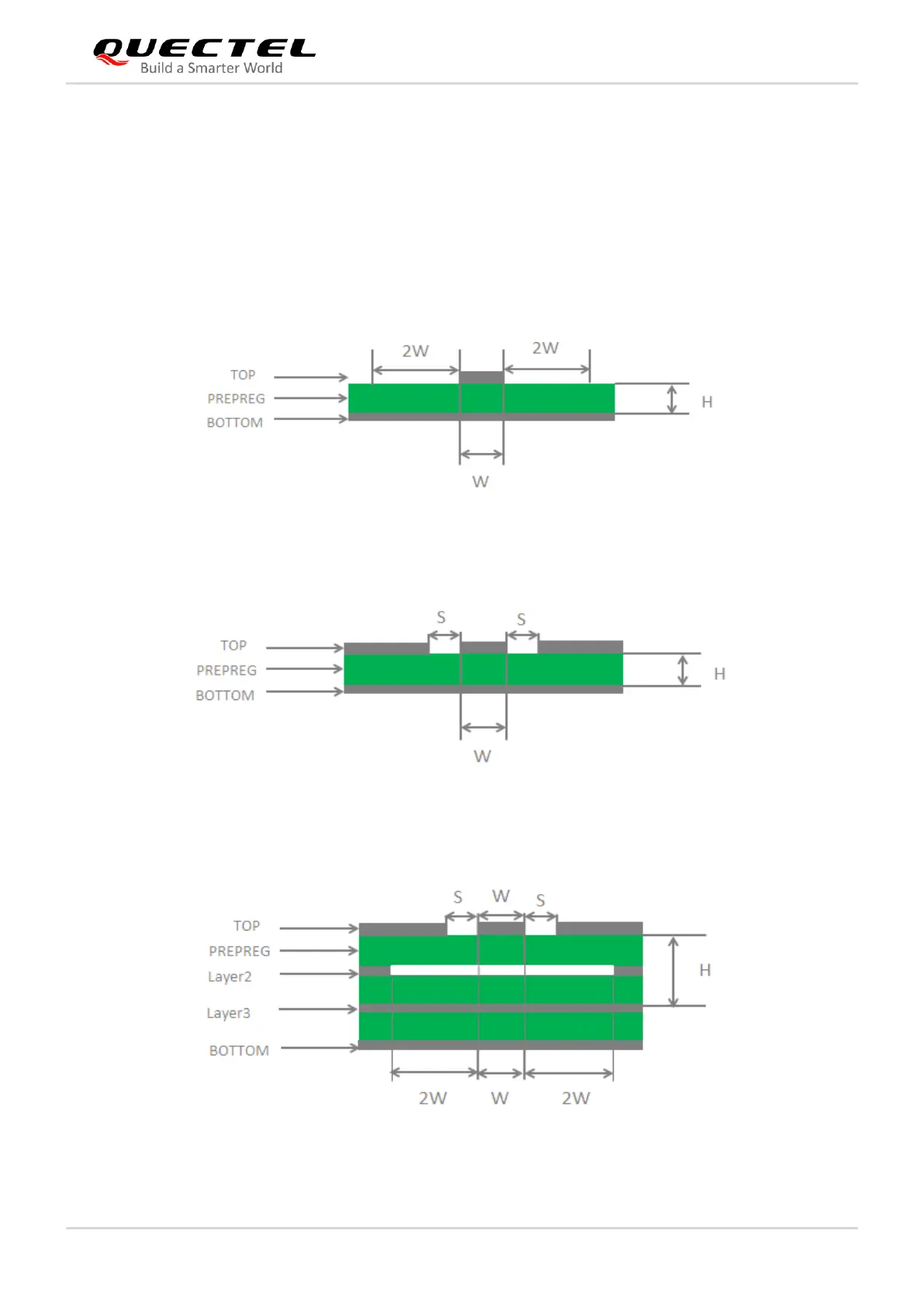
4.1.4. Reference Design of RF Layout
For the module to be applicable to your PCB, the characteristic impedance of all RF traces should be
controlled at 50 Ω. The impedance of the RF traces is usually determined by the trace width (W), the
materials’ dielectric constant, the height from the reference ground to the signal layer (H), and the spacing
between RF traces and grounds (S). Microstrip or coplanar waveguide is typically used in RF layout to
control characteristic impedance. The following are reference designs of microstrip or coplanar
waveguide with different PCB structures.
Figure 32: Reference Design of Microstrip on 2-layer PCB
Figure 33: Reference Design of Coplanar Waveguide on 2-layer PCB
Figure 34: Reference Design of Coplanar Waveguide on 4-layer PCB (Layer 3 as Reference
Ground)
 Loading...