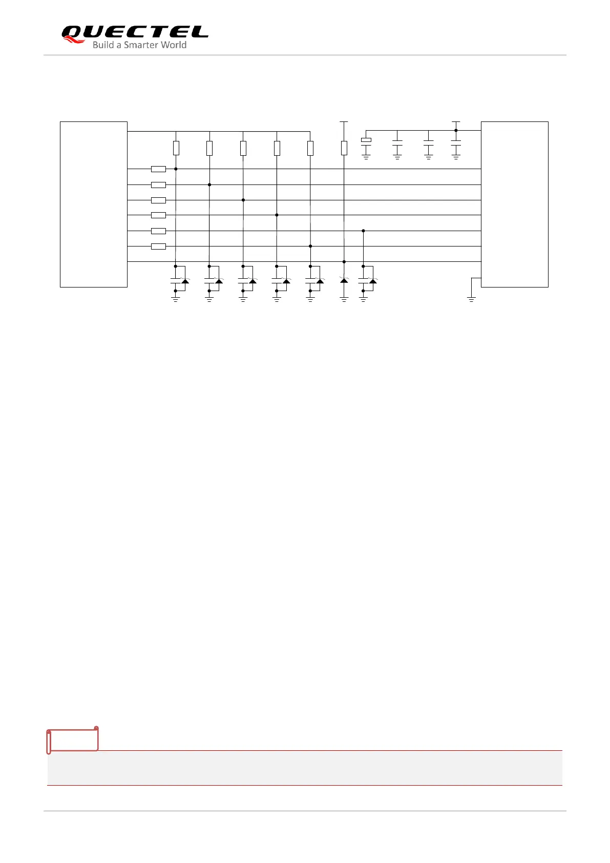
Figure 27: Reference Design of SD Card Interface
Please follow the principles below in SD card circuit design:
⚫ The voltage range of SD power supply VDD_3V3 is 2.7–3.6 V and a sufficient current of 0.8 A at least
should be provided. As the maximum output current of VDD_SDIO is 50 mA, which can only be used
for SDIO pull-up resistors, an external power supply is needed for SD card.
⚫ To avoid jitter of bus, resistors R7–R11 are needed to pull up the SDIO to SDIO_VDD. Value of these
resistors is among 10–100 kΩ and the recommended value is 100 kΩ.
⚫ In order to improve signal quality, it is recommended to add 0 ohm resistors R1–R6 in series between
the module and the SD card. The bypass capacitors C1–C6 are reserved and not mounted by default.
All resistors and bypass capacitors should be placed close to the module.
⚫ In order to offer good ESD protection, it is recommended to add a TVS diode on SD card pins.
⚫ The load capacitance of SDIO bus needs to be less than 40 pF.
⚫ It is important to route the SDIO signal traces with total grounding. The impedance of SDIO data
trace is 50 Ω (±10 %).
⚫ Keep SDIO signals far away from other sensitive circuits/signals, such as RF circuits, analog signals,
etc., as well as noisy signals, such as clock signals, DCDC signals, etc.
⚫ It is recommended to keep the trace length difference between CLK and DATA/CMD less than 1 mm
and the total routing length less than 50 mm. The total trace length inside the module is 36 mm, so
the exterior total trace length should be less than 14 mm.
⚫ Make sure the spacing between adjacent traces is two times of the trace width and that the load
capacitance of SDIO bus is less than 40 pF.
 Loading...