9. Interrupts
puorG92/C61M
page 86
854fo7002,03.raM21.1.veR
2110-1010B90JER
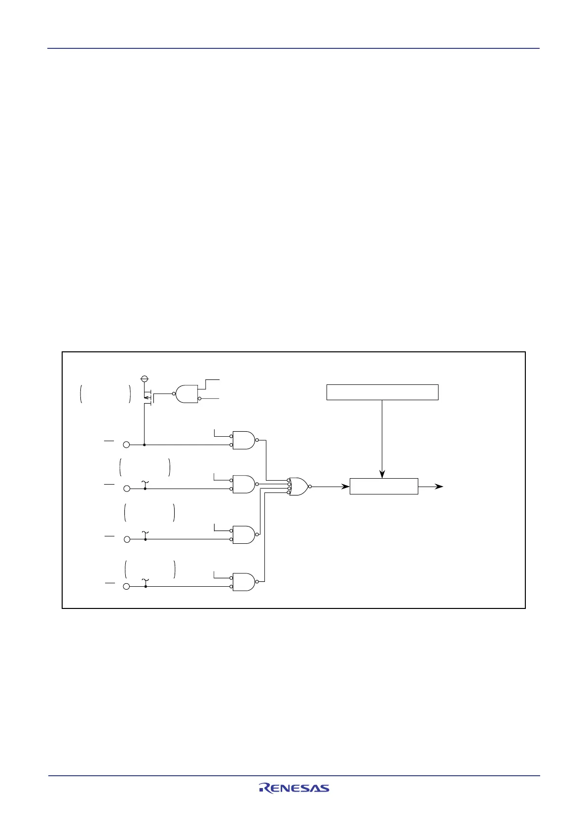
Interrupt control circuit
KUPIC register
Key input interrupt
request
KI
3
KI
2
KI
1
KI
0
PU25 bit in the PUR2
register
PD10_7 bit in the
PD10 register
Pull-up
transistor
PD10_7 bit in the PD10 register
PD10_6 bit in the
PD10 register
PD10_5 bit in the
PD10 register
PD10_4 bit in the
PD10 register
Pull-up
transistor
Pull-up
transistor
Pull-up
transistor
______
9.7 NMI Interrupt
_______ _______
An NMI interrupt request is generated when input on the NMI pin changes state from high to low, after the
_______ ______
NMI interrupt was enabled by writing a 1 to bit 4 in the register PM2. The NMI interrupt is a non-maskable
interrupt, once it is enabled.
_______
The input level of this NMI interrupt input pin can be read by accessing the P8_5 bit in the P8 register.
_______
NMI is disabled by default after reset (the pin is a GPIO pin, P85) and can be enabled using bit 4 in the PM2
register. Once enabled, it can only be disabled by a reset signal.
_______
The NMI input has a digital debounce function for noise rejection. Refer to "19.6 Digital Debounce func-
_______
tion" for details. When using NMI interrupt to exit stop mode, set the NDDR register to FF16 before entering
stop mode.
9.8 Key Input Interrupt
A key input interrupt is generated when input on any of the P104 to P107 pins which has had bits PD10_7 to
PD10_4 in the PD10 register set to 0 (= input) goes low. Key input interrupts can be used for a key-on
wakeup function to get the MCU to exit stop or wait modes. However, if you intend to use the key input
interrupt, do not use P104 to P107 as analog input ports. Figure 9.12 shows the block diagram of the key
input interrupt. Note, however, that while input on any pin which has had bits PD10_7 to PD10_4 set to 0 (=
input mode) is pulled low, inputs on all other pins of the port are not detected as interrupts.
Figure 9.12 Key Input Interrupt
 Loading...


