20. Flash Memory Version
puorG92/C61M
page 365
854fo7002,03.raM21.1.veR
2110-1010B90JER
CAN_H
CAN_L
P92/CRx
SCLK
T
X
D
CNVss
P8
6
(CE)
RESET
P93/CTx
Reset input
User reset
singnal
MCU
(1) Control pins and external circuits vary with the CAN programmer.
For more information, refer to the user's manual include with the CAN programmer.
(2) In this example, a selector controls the input voltage applied to CNVss to switch
between single-chip mode and CAN I/O mode.
P8
5
(RP)
(Note 1)
(Note 1)
CAN transceiver
P1
6
(Note 1)
Note 1. Set following either or both.
•Connect the CE pin to V
CC
•Connect the RP pin to V
SS
and the P1
6
pin to V
CC
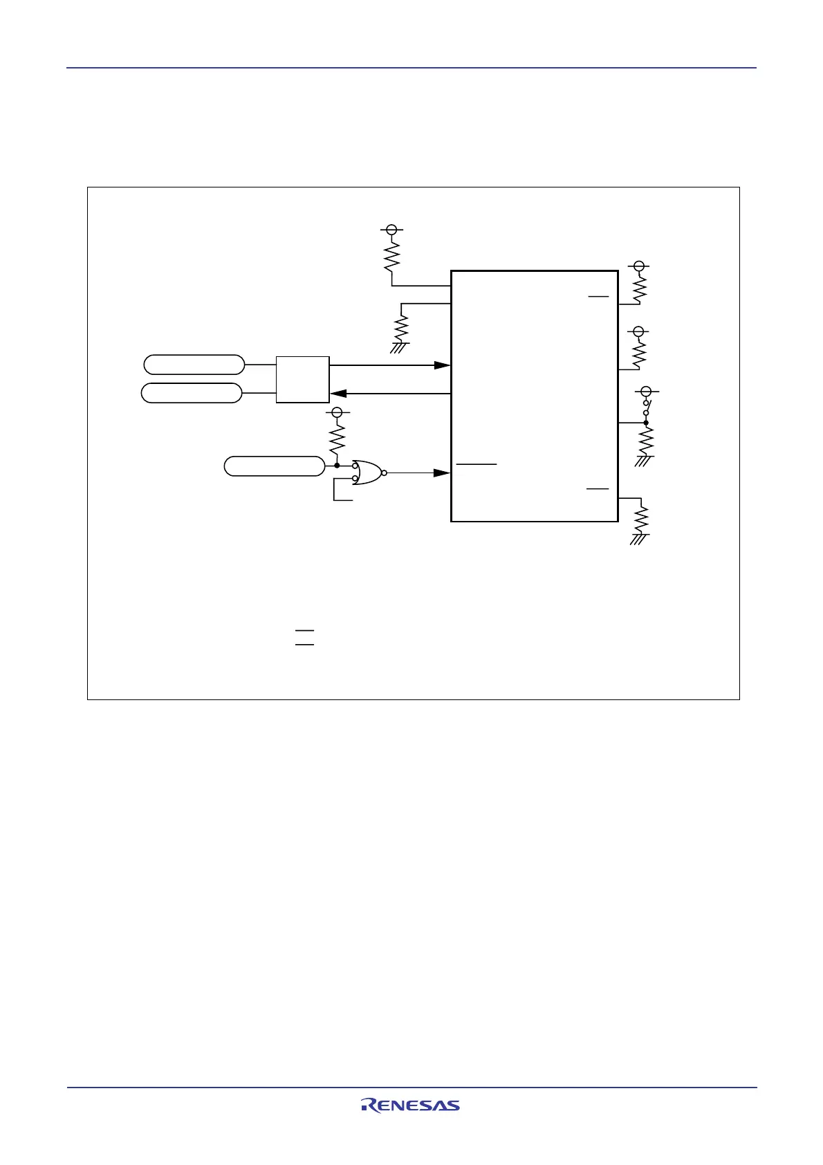
20.11.2 Example of Circuit Application in CAN I/O Mode
Figure 20.21 shows example of circuit application in CAN I/O mode. Refer to the user’s manual for CAN
programmer to handle pins controlled by a CAN programmer.
Figure 20.21 Circuit Application in CAN I/O Mode
 Loading...


