20. Flash Memory Version
puorG92/C61M
page 358
854fo7002,03.raM21.1.veR
2110-1010B90JER
SCLK input
BUSY output
TxD output
RxD input
BUSY
SCLK
TXD
CNVss
P86(CE)
RESET
RxD
Reset input
User reset
singnal
MCU
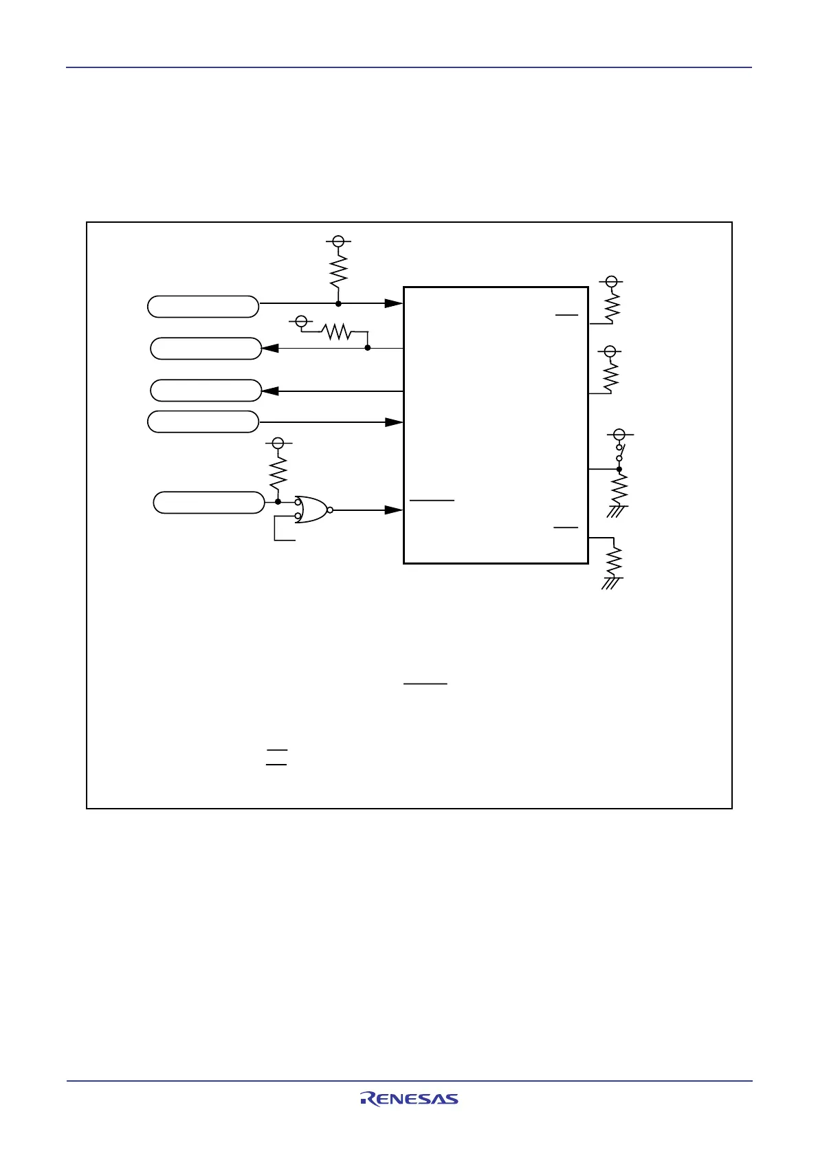
(1) Controlling pins and external circuits vary with the serial programmer. For more
information, refer to the user's manual included with the serial programmer.
(2) In this example, a selector controls the input voltage applied to CNVss to switch
between single-chip mode and standard serial I/O mode.
(3) In standard serial input/output mode 1, if the user reset signal becomes “L” while
the MCU is communicating with the serial programmer, break the connection
between the user reset signal and the RESET pin using a jumper switch.
P85(RP)
(1)
(1)
NOTE:
1. Set the following, either or both.
- Connect the CE pin to Vcc
- Connect the RP pin to Vss and the P16 pin to Vcc
(1)
P16
20.9.2 Example of Circuit Application in Standard Serial I/O Mode
Figure 20.17 shows an example of a circuit application in standard serial I/O mode 1 and Figure 20.18
shows an example of a circuit application in standard serial I/O mode 2. Refer to the user's manual of your
serial programmer to handle pins controlled by the serial programmer.
Figure 20.17 Circuit Application in Standard Serial I/O Mode 1
 Loading...


