14. Serial I/O
puorG92/C61M
page 220
854fo7002,03.raM21.1.veR
2110-1010B90JER
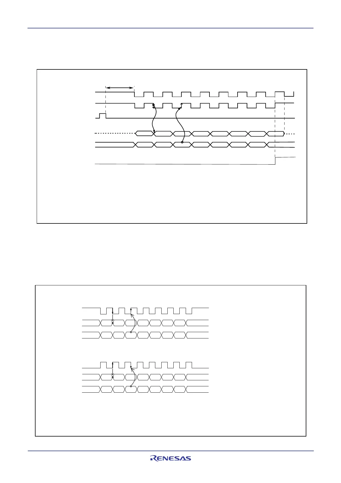
14.2.1 SI/Oi Operation Timing
Figure 14.37 shows the SI/Oi operation timing
Figure 14.37 SI/Oi Operation Timing
14.2.2 CLK Polarity Selection
The the SMi4 bit in the SiC register allows selection of the polarity of the transfer clock. Figure 14.38
shows the polarity of the transfer clock.
Figure 14.38 Polarity of Transfer Clock
D7D0 D1 D2 D3 D4 D5 D6
i= 3, 4
1.5 cycle (max)
SI/Oi internal clock
CLKi output
Signal written to the
SiTRR register
S
OUTi output
S
INi input
SiIC register
IR bit
(2)
"H"
"L"
"H"
"L"
"H"
"L"
"H"
"L"
"H"
"L"
1
0
(3)
NOTES:
1. This diagram applies to the case where the SiC register bits are set as follows:
SMi2 = 0 (S
OUTi output), SMi3 = 1 (SOUTi output, CLKi function), SMi4 = 0 (transmit data output at the falling edge and receive data input at the
rising edge of the transfer clock), SMi5 = 0 (LSB first) and SMi6 = 1 (internal clock)
2. When the SMi6 bit is set to 0 (internal clock), the S
OUTi pin is placed in the high-impedance state after the transfer is completed.
3. If the SMi6 bit is set to 0 (internal clock), the serial I/O starts sending or receiving data a maximum of 1.5 transfer clock cycles after writing to
the SiTRR register.
(2) When the SMi4 bit in the SiC register is set to 1
(3)
D
1 D2 D3 D4 D5 D6 D7
D1 D2 D3 D4 D5 D6 D7
D0
D0
SINi
SOUTi
CLKi
(1) When the SMi4 bit in the SiC register is set to 0
D1 D2 D3 D4 D5 D6 D7D0
D1 D2 D3 D4 D5 D6 D7D0
SINi
SOUTi
CLKi
(2)
i=3 and 4
NOTES:
1. This diagram applies to the case where the SiC register bits are set as follows:
SMi5 = 0 (LSB first) and SMi6 = 1 (internal clock)
2. When the SMi6 bit is set to 1 (internal clock), a high level is output from the CLKi pin if not transferring data.
3 When the SMi6 bit is set to 1 (internal clock), a low level is output from the CLKi pin if not transferring data.
 Loading...


