20. Flash Memory Version
puorG92/C61M
page 347
854fo7002,03.raM21.1.veR
2110-1010B90JER
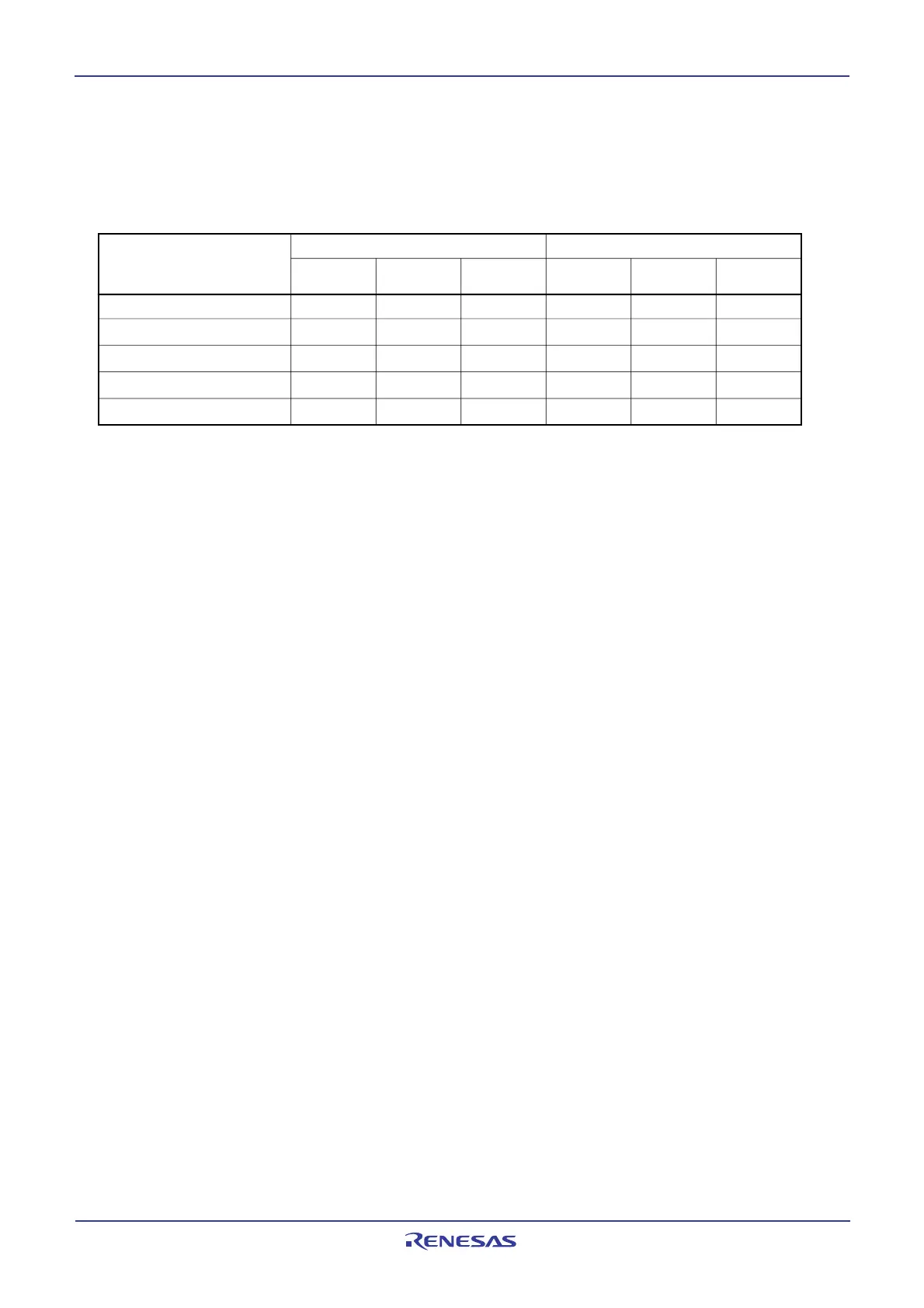
Command
Program
Clear status register
Read array
Read status register
First bus cycle Second bus cycle
Block erase
Write
Write
Write
Write
Write
Mode
Read
Write
Write
Mode
X
WA
BA
Address
SRD
WD
xxD0
16
Data
(D
15
to D
0
)
xxFF
16
xx70
16
xx50
16
xx40
16
xx20
16
Data
(D
15
to D
0
)
X
X
X
WA
X
Address
SRD: Status register data (D
7
to D
0
)
WA : Write address (However,even address)
WD : Write data (16 bits)
BA : Highest-order block address (However,even address)
X : Any even address in the user ROM area
xx : 8 high-order bits of command code (ignored)
20.7 Software Commands
Read or write 16-bit commands and data from or to even addresses in the user ROM area. When writing a
command code, 8 high-order bits (D15–D8) are ignored.
Table 20.5 Software Commands
20.7.1 Read Array Command (FF16)
The read array command reads the flash memory.
Read array mode is entered by writing command code xxFF16 in the first bus cycle. Content of a speci-
fied address can be read in 16-bit unit after the next bus cycle. The MCU remains in read array mode until
an another command is written. Therefore, contents of multiple addresses can be read consecutively.
20.7.2 Read Status Register Command (7016)
The read status register command reads the status register.
By writing command code xx7016 in the first bus cycle, the status register can be read in the second bus
cycle (Refer to 20.8 Status Register). Read an even address in the user ROM area. Do not execute this
command in EW mode 1.
20.7.3 Clear Status Register Command (5016)
The clear status register command clears the status register to 0.
By writing xx5016 in the first bus cycle, and bits FMR06 to FMR07 in the FMR0 register and bits SR4 to
SR5 in the status register are set to 0.
 Loading...


