12. Timer A
puorG92/C61M
page 108
854fo7002,03.raM21.1.veR
2110-1010B90JER
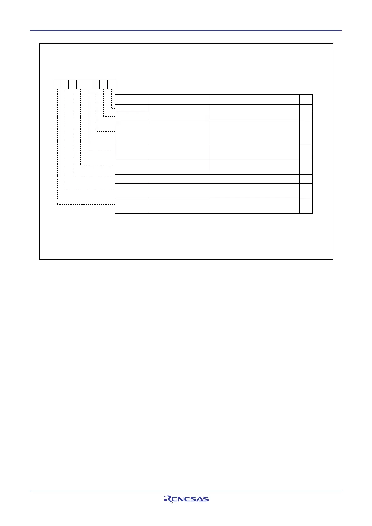
Figure 12.8 TAiMR Register in Event Counter Mode (when not using two-phase pulse signal
processing)
Symbol Address After Reset
TA0MR to TA4MR 0396
16 to 039A16 0016
WR
b7 b6 b5 b4 b3 b2 b1 b0
Operation mode select bit
0 1 : Event counter mode
(1)
b1 b0
TMOD0
MR0
0: Pulse is not output
(TA
iOUT pin functions as I/O port)
1: Pulse is output
(TAiOUT pin functions as pulse output pin)
MR2
MR1
MR3 Set to 0 in event counter mode
TCK0
Count operation type
select bi
t
010
0: Counts external signal's falling edge
1: Counts external signal's rising edge
Up/down switching
cause select bit
0: Reload type
1: Free-run type
Bit Symbol Bit Name Function
RW
TCK1 Can be 0 or 1 when not using two-phase pulse signal processing
TMOD1
Timer Ai Mode Register (i=0 to 4)
(When not using two-phase pulse signal processing)
RW
RW
RW
RW
RW
RW
RW
RW
NOTES:
1. During event counter mode, the count source can be selected using registers ONSF and TRGSR.
2. Effective when bits TAiTGH and TAiTGL in the ONSF or TRGSR register are 00
2 (TAiIN pin input).
3. Decrement when input on TAi
OUT pin is low or increment when input on that pin is high. The port
direction bit for TAi
OUT pin must be set to 0 (input mode).
Pulse output function
select bit
Count polarityselect bit
(2)
0: UDF register
1: Input signal to TA
iOUT pin
(3)
 Loading...


