13. Timer S
puorG92/C61M
page 141
854fo7002,03.raM21.1.veR
2110-1010B90JER
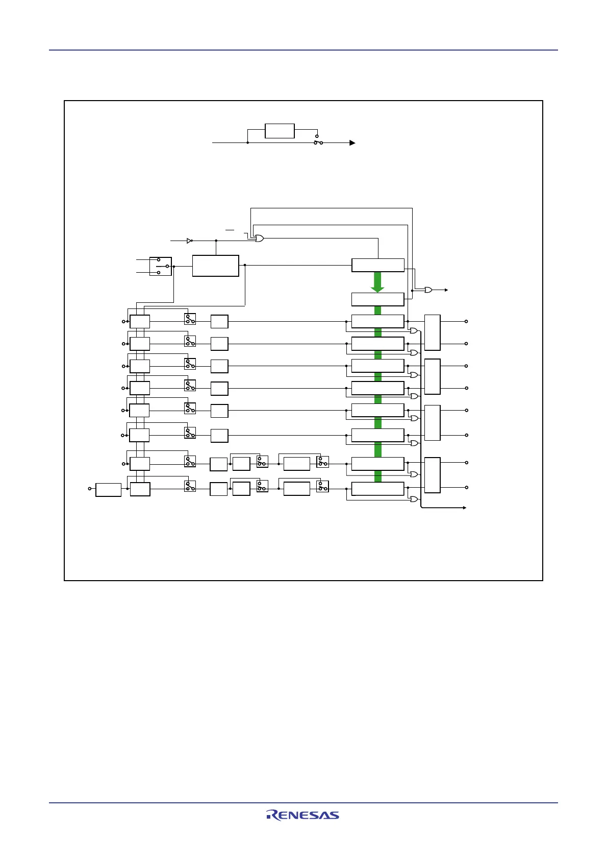
Figure 13.1 IC/OC Block Diagram
BTS: Bits in the G1BCR1 register
CTS1 to CTS0, DF1 to DF0, GT, PR : Bits in the G1TMCRj register (j= 0 to 7)
PCLK0 : Bits in the PCLKR register
G1TM0, G1PO0
register
G1TM1, G1PO1
register
G1TM2, G1PO2
register
G1TM3, G1PO3
register
G1TM4, G1PO4
register
G1TM5, G1PO5
register
G1TM6, G1PO6
register
G1TM7, G
1PO
7
register
PWM
output
PWM
output
PWM
output
PWM
output
Base timer reset
(n+1)
Divider register
Edge
select
Digital
filter
Gate
functio
n
Edge
select
Digital
filter
Gate
function
Edge
select
Digital
filter
Edge
select
Digital
filter
INPC1
0
INPC1
1
INPC1
6
(G1DV)
GT
GT
PR
PR
Ch0 to ch7
interrupt request signal
OUTC1
0
OUTC1
1
OUTC1
4
OUTC1
5
Prescaler
function
Prescaler
function
OUTC1
6
OUTC1
7
OUTC1
2
OUTC1
3
(Note 1)
Base timer
f
BT1
Edge
select
Digital
filter
INPC1
2
Two-phase
pulse input
BCK1 to BCK0 : Bits in the G1BCR0 register
Request from INT1 pi
n
BTS
Request by matching G1PO0 register and base timer
Base timer over flow request
BCK1 to BCK0
11
10
00
10:f
BT1
11: f
1
or f
2
DF1 to DF0
CTS1 to CTS0
CTS1 to CTS0
CTS1 to CTS0
00
DF1 to DF0
00
DF1 to DF0
00
DF1 to DF0
00
0
0
1
0
1
0
1
1
DF1 to DF0
Base timer reset
register (G1BTRR)
Request by matching G1BTRR and base timer
00
CTS1 to CTS0
DF1 to DF0
Edge
select
Digital
filter
INPC1
3
DF1 to DF0
Edge
select
Digital
filter
INPC1
4
CTS1 to CTS0
DF1 to DF0
Edge
select
Digital
filter
INPC1
5
CTS1 to CTS0
INPC1
7
Digital
debounce
Base timer reset request
Base timer interrupt request
00
00
CTS1 to CTS0
CTS1 to CTS0
1/2
PCLK0=0
PCLK0=1
f
1
or f
2
f
1
or f
2
Main clock,
PLL clock,
On-chip
oscillator clock
10:f
BT1
11: f
1
or f
2
10:f
BT1
11: f
1
or f
2
10:f
BT1
11: f
1
or f
2
10:f
BT1
11: f
1
or f
2
10:f
BT1
11: f
1
or f
2
10:f
BT1
11: f
1
or f
2
10:f
BT1
11: f
1
or f
2
Figure 13.1 shows the block diagram of the IC/OC.
 Loading...


