15. A/D Converter
puorG92/C61M
page 249
854fo7002,03.raM21.1.veR
2110-1010B90JER
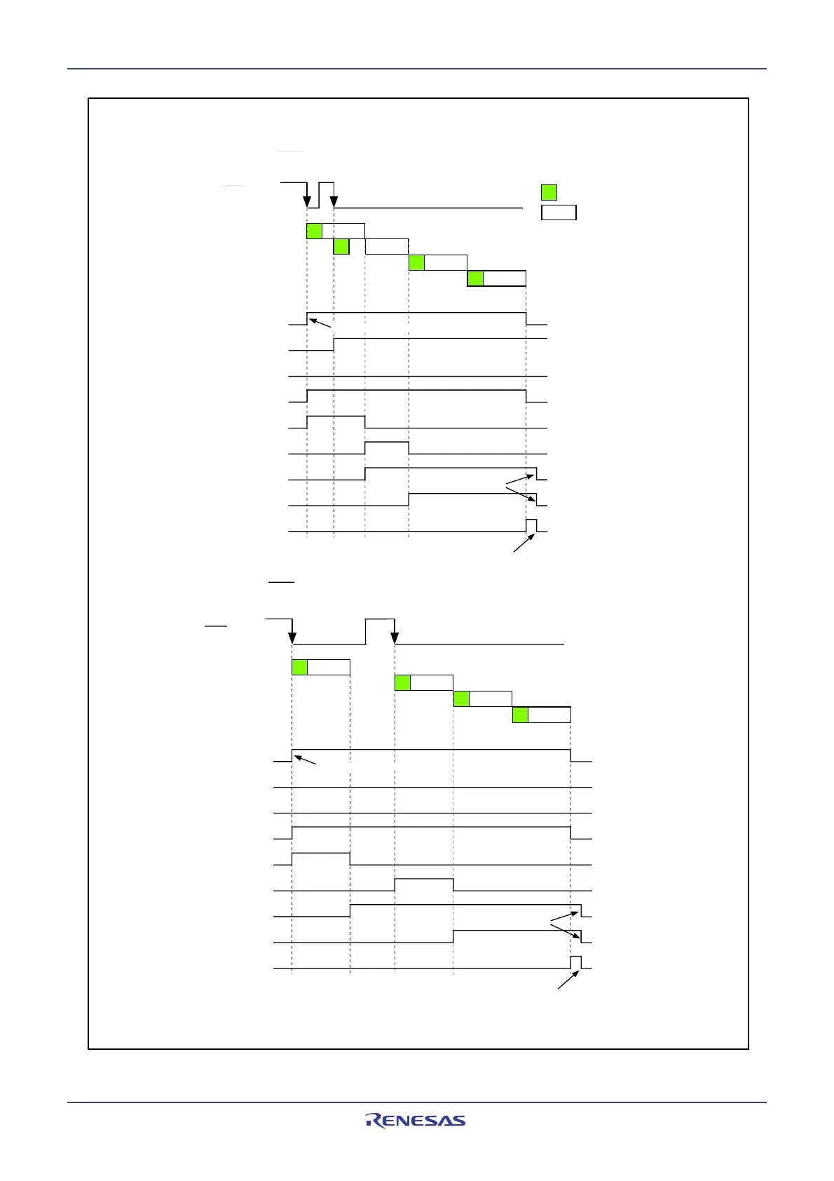
Figure 15.25 Each Flag Operation in ADSTAT0 Register Associated with the Operation Example
in Delayed Trigger Mode 1 (1)
•Example when selecting AN
0
to AN
3
to A/D sweep pins (SCAN1 to SCAN0 = 01
2
)
A/D pin input
voltage sampling
A/D pin conversion
AN
0
AN
1
AN
2
AN
3
AD
TRG
pin input
•Example 1: When AD
TRG
pin falling edge is generated during AN
0
pin conversion
ADST flag
ADERR0 flag
ADERR1 flag
ADTCSF flag
ADSTT0 flag
ADSTT1 flag
ADSTRT0 flag
ADSTRT1 flag
IR bit in the ADIC
register
1
0
1
0
1
0
1
0
1
0
1
0
1
0
1
0
1
0
Set to 0 b
interru
t re
uest acknowled
ement or a
ro
ram
Set to 0 by program
Do not set to 1 by program
AN
0
AN
1
AN
2
AN
3
•Example 2: When AD
TRG
pin falling edge is generated again after AN
0
pin conversion
ADST flag
ADERR0 flag
ADERR1 flag
ADTCSF flag
ADSTT0 flag
ADSTT1 flag
ADSTRT0 flag
ADSTRT1 flag
IR bit in the ADIC
register
1
0
1
0
1
0
1
0
1
0
1
0
1
0
1
0
1
0
ADST flag: Bit 6 in the ADCON0 register
ADERR0, ADERR1, ADTCSF, ADSTT0, ADSTT1, ADSTRT0 and ADSTRT1 flag: bits 0, 1, 3, 4, 5, 6 and 7 in the ADSTAT0 register
Set to 0 by interrupt request acknowledgment or a program
Set to 0 by program
Do not set to 1 by program
AD
TRG
pin input
 Loading...


