19. Programmable I/O Ports
puorG92/C61M
page 329
854fo7002,03.raM21.1.veR
2110-1010B90JER
Table 19.1 Unassigned Pin Handling in Single-chip Mode
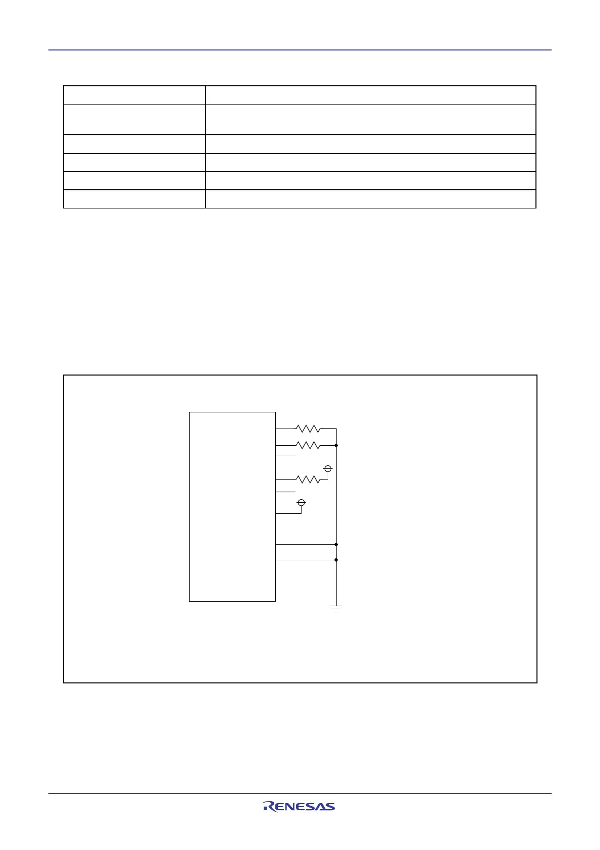
Figure 19.13 Unassigned Pin Handling
(Input mode)
·
·
·
(Input mode)
(Output mode)
X
OUT
AV
CC
AV
SS
V
ref
MCU
V
CC
V
SS
In single-chip mode
Open
Open
·
·
·
(1)
Port P0 to P3, P6 to P10
X
IN
NOTE:
1. When using the 64-pin package, set bits PACR2, PACR1, and PACR0 to 010
2
.
When using the 80-pin package, set bits PACR2, PACR1, and PACR0 to 011
2
.
emaNniPgnitteS
01Pot6P,3Pot0PstroP VotniphcaetcennocdnaedomtupniretnE
SS ;)nwod-llup(rotsiseraaiv
neposnipehtevaeldnaedomtuptuoretnero
)4,2,1(
X TUO neponipevaeL
)3(
X NI VotniptcennoC CC )pu-llup(rotsiseraaiv
)5(
VA CC VotniptcennoC CC
VA SS V, FER VotniptcennoC SS
NOTES:
1. If the port enters output mode and is left open, it is in input mode before output mode is entered by program
after reset. While the port is in input mode, voltage level on the pins is indeterminate and power consumption
may increase. Direction register setting may be changed by noise or failure caused by noise. Configure
direction register settings regulary to increase the reliability of the program.
2. Use the shortest possible wiring to connect the MCU pins to unassigned pins (within 2 cm).
3. When the external clock is applied to the XIN pin, set the pin as written above.
4. In the 64-pin package, set bits PACR2, PACR1, and PACR0 in the PACR register to 010
2. In the 80-pin
package, set bits PACR2, PACR1, and PACR0 to 0112.
5. When the main clock oscillation is not used, set the CM05 bit in the CM0 register to 1 (main clock stops) to
reduce power consumption.
 Loading...


