20. Flash Memory Version
puorG92/C61M
page 355
854fo7002,03.raM21.1.veR
2110-1010B90JER
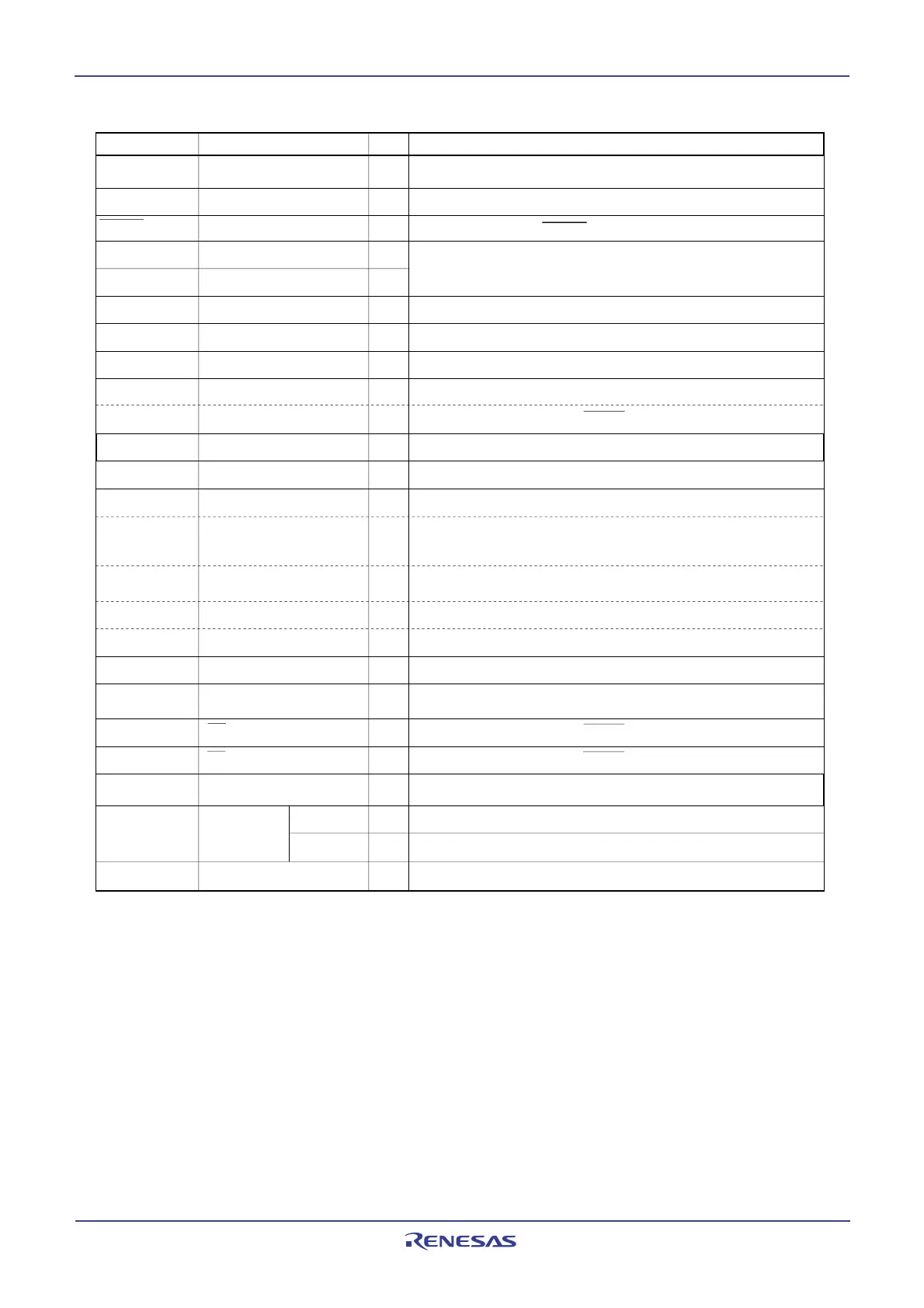
Table 20.8 Pin Descriptions (Flash Memory Standard Serial I/O Mode)
NOTES:
___________
1. When using standard serial I/O mode 1, to input “H” to the TxD pin is necessary while the RESET pin is held “L”.
Therefore, connect this pin to V
CC via a resistor. Adjust the pull-up resistor value on a system not to affect a data
transfer after reset, because this pin changes to a data-output pin
2. Set the following, either or both.
_____
-Connect the CE pin to VCC.
_____
-Connect the RP pin to VSS and P16 pin to VCC.
Pin Descriptio
n
V
CC
,V
SS
Apply the voltage guaranteed for Program and Erase to Vcc pin and 0
V to Vss pin.
CNV
SS
Connect to Vcc pin.
RESET
X
IN
Connect a ceramic resonator or crystal oscillator between X
IN
and
X
OUT
pins. To input an externally generated clock, input it to X
IN
pin
and open X
OUT
pin.
X
OUT
AV
CC
, AV
SS
V
REF
Connect AVss to Vss and AVcc to Vcc, respectively.
Enter the reference voltage for AD conversion.
P0
0
to P0
7
Input “H” or “L” signal or leave open.
P1
0
to P1
5
, P1
7
Input “H” or “L” signal or leave open.
P3
0
to P3
7
Input "H" or “L” level signal or leave open.
P6
0
to P6
3
Input "H" or “L” level signal or leave open.
P6
4
Standard serial I/O mode 1: BUSY signal output pin
Standard serial I/O mode 2: Monitor signal output pin for boot program
operation check
P6
5
P6
6
Serial data input pin
P6
7
Serial data output pin
P7
0
to P7
7
Input “H” or “L” signal or leave open.
P8
0
to P8
4
,
P8
7
Input “H” or “L” signal or leave open.
P9
0
to P9
2
,
P9
5
to P9
7
Input “H” or “L” signal or leave open.
Name
Power input
CNV
S
S
Reset input
Clock input
Clock output
Analog power supply input
Reference voltage input
Input port P0
Input port P1
Input port P3
Input port P6
BUSY output
SCLK input
RxD input
TxD output
Input port P7
Input port P8
Input port P9
I/O
I
I
I
O
I
I
I
I
I
O
I
I
O
I
I
I
P10
0
to P10
7
Input “H” or “L” signal or leave open.Input port P10 I
P8
5
RP input I
Connect this pin to Vss while RESET pin is “L”.
(2)
Standard serial I/O mode 1: Serial clock input pin
Standard serial I/O mode 2: Input “L”.
Reset input pin. While RESET pin is “L”, wait for td(ROC).
(1)
P2
0
to P2
7
Input port P2 Input "H" or “L” level signal or leave open.I
P8
6
CE input
I
Connect this pin to Vcc while RESET pin is “L”.
(2)
P1
6
Input port P1 I
Connect this pin to Vcc while RESET pin is “L”.
(2)
P9
3
Input “H” or “L” signal or leave open.
Input port P9
3
I
“H” signal is output for specific time. Input “H” signal or leave open.I/O
T-ver./V-ver.
Normal-ver.
 Loading...


