20. Flash Memory Version
puorG92/C61M
page 362
854fo7002,03.raM21.1.veR
2110-1010B90JER
Pin Description
V
CC
,V
SS
Apply the voltage guaranteed for Program and Erase to Vcc pin and 0
V to Vss pin.
CNV
SS
Connect to Vcc pin.
RESET
X
IN
Connect a ceramic resonator or crystal oscillator between X
IN
and
X
OUT
pins. To input an externally generated clock, input it to X
IN
pin
and open X
OUT
pin.
X
OUT
AV
CC
, AV
SS
V
REF
Connect AVss to Vss and AVcc to Vcc, respectively.
Enter the reference voltage for AD from this pin.
P0
0
to P0
7
Input "H" or "L" level signal or leave open.
P1
0
to P1
5
, P1
7
Input "H" or "L" level signal or leave open.
P3
0
to P3
7
Input "H" or "L" level signal or leave open.
P6
0
to P6
4
, P6
6
Input "H" or "L" level signal or leave open.
P6
5
P6
7
Input "H" level signal.
P7
0
to P7
7
Input "H" or "L" level signal or leave open.
P8
0
to P8
4
,
P8
7
Input "H" or "L" level signal or leave open.
P9
0
to P9
1
,
P9
5
to P9
7
Input "H" or "L" level signal or leave open.
P10
0
to P10
7
Input "H" or "L" level signal or leave open.
Name
Power input
CNV
SS
Reset input
Clock input
Clock output
Analog power supply input
Reference voltage input
Input port P0
Input port P1
Input port P3
Input port P6
SCLK input
TxD output
Input port P7
Input port P8
Input port P9
Input port P10
I/O
I
I
I
O
I
I
I
I
I
I
O
I
I
I
I
P8
5
RP input I Connect this pin to Vss while RESET is low. (Note 1)
Input "L" level signal.
Reset input pin. While RESET pin is "L" level, wait for td(ROC).
P2
0
to P2
7
Input port P2 Input "H" or "L" level signal or leave open.I
P8
6
CE input
I Connect this pin to Vcc while RESET is low. (Note 1)
P9
2
Connect this pin to a CAN transceiver.
P9
3
Connect this pin to a CAN transceiver.
CRX input
CTX output
I
O
Connect this pin to Vcc while RESET is low. (Note 1)P1
6
Input port P1 I
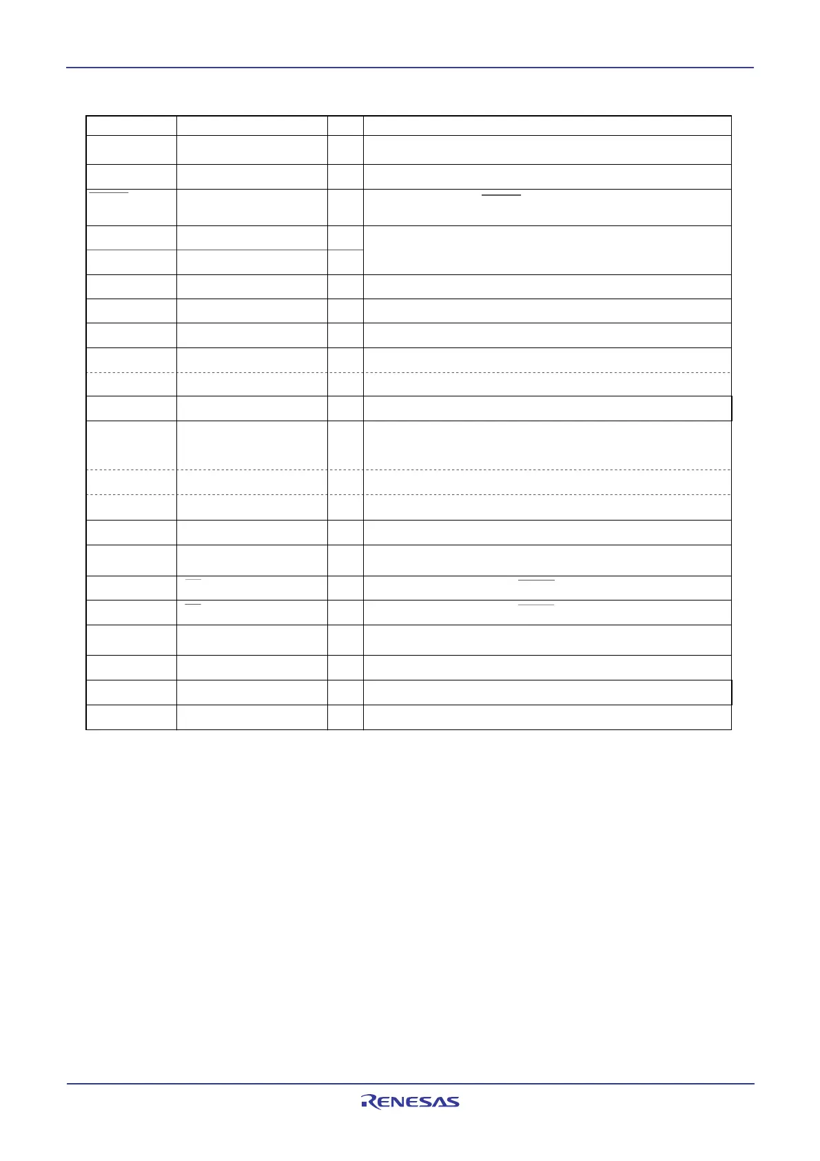
Table 20.9 Pin Functions for CAN I/O Mode
NOTE:
1. Set following either or both.
_____
•Connect the CE pin to VCC.
_____
•Connect the RP pin to VSS and the P16 pin to VCC.
 Loading...


