7. Clock Generation Circuit
page 49
854fo7002,03.raM21.1.veR
2110-1010B90JER
puorG92/C61M
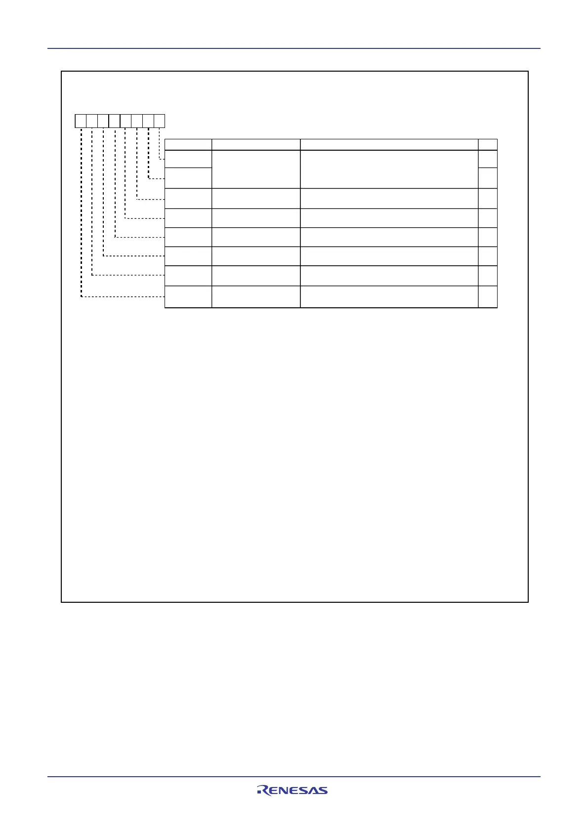
Figure 7.2 CM0 Register
System Clock Control Register 0
(1)
Bit Name FunctionBit Symbol
b7 b6 b5 b4 b3 b2 b1 b0
CM07
CM05
CM04
CM03
CM02
CM06
Wait Mode peripheral function
clock stop bit
(10)
0: Do not stop peripheral function clock in wait mode
1: Stop peripheral function clock in wait mode
(8)
X
CIN
-X
COUT
drive capacity
select bit
(2)
0: LOW
1: HIGH
0: I/O port P8
6
, P8
7
1: X
CIN
-X
COUT
generation function
(9)
Main clock stop bit
(3, 10, 12, 13)
0: On
(4)
1: Off
(5)
Main clock division select
bit 0
(7, 13, 14)
0: CM16 and CM17 valid
1: Division by 8 mode
System clock select bit
(6, 10, 11, 12)
0: Main clock, PLL clock, or on-chip oscillator clock
1: Sub-clock
RW
Port X
C
select bit
(2)
RW
RW
RW
RW
RW
RW
RW
Clock output function
select bit
See Table 7.3
CM00
CM01
RW
NOTES:
1. Write to this register after setting the PRC0 bit in the PRCR register to 1 (write enable).
2. The CM03 bit is set to 1 (high) when the CM04 bit is set to 0 (I/O port) or the MCU goes to a stop mode.
3. This bit is provided to stop the main clock when the low power dissipation mode or on-chip oscillator low power dissipation mode
is selected. This bit cannot be used for detection as to whether the main clock stopped or not. To stop the main clock, the
following setting is required:
(1) Set the CM07 bit to 1 (Sub-clock select) or the CM21 bit in the CM2 register to 1 (on-chip oscillator select) with the sub-
clock stably oscillating.
(2) Set the CM20 bit in the CM2 register to 0 (Oscillation stop, re-oscillation detection function disabled).
(3) Set the CM05 bit to 1 (Stop).
4. During external clock input, set the CM05 bit to 0 (On).
5. When CM05 bit is set to 1, the X
OUT
pin goes "H". Futhermore, because the internal feedback resistor remains connectes,
the X
IN
pin is pulled "H" to the same level as X
OUT
via the feedback resistor.
6. After setting the CM04 bit to 1 (X
CIN
-X
COUT
oscillator function), wait until the sub-clock oscillates stably before switching
the CM07 bit from 0 to 1 (sub-clock).
7. When entering stop mode from high or middle speed mode, on-chip oscillator mode or on-chip oscillator low power mode, the
CM06 bit is set to 1 (divided-by-8 mode).
8. The f
C32
clock does not stop. During low speed or low power dissipation mode, do not set this bit to 1(peripheral clock turned
off in wait mode).
9. To use a sub-clock, set this bit to 1. Also, make sure ports P8
6
and P8
7
are directed for input, with no pull-ups.
10. When the PM21 bit in the PM2 register is set to 1 (clock modification disable), writing to bits CM02, CM05, and CM07 has
no effect.
11. If the PM21 bit needs to be set to 1, set the CM07 bit to 0 (main clock) before setting it.
12. To use the main clock a the clock source for the CPU clock, follow the procedure below.
(1) Set the CM05 bit to 0 (oscillate).
(2) Wait the main clock oscillation stabilized.
(3) Set all bits CM11, CM21, and CM07 to 0.
13. When the CM21 bit is set to 0 (on-chip oscillaor turned off) and the CM05 bit is set to 1 (main clock turned off), the CM06 bit
is fixed to 1 (divide-by-8 mode) and the CM15 bit is fixed to 1 (drive capability High).
14. To return from on-chip oscillator mode to high-speed or middle-speed mode set both bits CM06 and CM15 to 1.
Symbol Address After Reset
CM0 01001000
2000616
 Loading...


