Theory of Operation—465B Service
oscillator (once each
cycle) effectively performing
a
divide-by-two.
Therefore, the CHOP frequency is
ap-
proximately 500 kilohertz. The CHOP clock oscillator will
not
be
enabled
unless more than one input is selected. As
stated previously,
a single-input VERT MODE selection
will cause Ui 705
to remain in a state that will allow only the
selected input to
be
passed
on to the Delay Line Driver.
If multiple inputs are
selected for display,
U1705
will
be
clocked
to select the appropriate inputs
programmed for
display Transistors
Q1619,
Q1719, Q1617, and Q1636 (if
ADD ie
selected) arc being switched
at
the
Chop clock
frequency (CHOP
Mode). As the displays
are being
incremented,
the
O
0. Qi,
and
Q
2
outputs of U1705 are
being
used as state indicators tothe
Ao, A,, and Aj i nputs of
ROM U1605
to indicate the next input
to be
selected
for
display. The order
of priority of the switching
is: CH
1.
CH
2,
ADD, then TRIG
VIEW.
ALTERNATE
TRACE SYNC. With ALT Vertical Mode
selected, a HI
will
be present at U1905D pin 12. If more
than a single-input
display
is selected, a HI will also be
present
at pin 13. The CHOP clock will
then be disabled.
U
1905
A
will
be enabled to pass the Alternate Trace
Sync
pulse to
U 1 805C pi n
9,
and U
1
805C will
be
enabled
to pass
the pulse
to U1705 pin
9
(clock input).
U1705 will now be
switching
between selected inputs at
a
rate
determined by
the Alternate
Trace Sync pulse
from the Horizontal
Display Logic
circuit.
If a single input is selected for display, UI 805B pin 5 will
be
LO and the Chop clock will remain disabled. The
Alternate Trace Sync pulse will
be
present at U1705pin9,
but with
only
one input
selected
by the
VERT
MODE
switches, U1705 will not change state and the switching
transistor for the selected input to
be
displayed will remain
on.
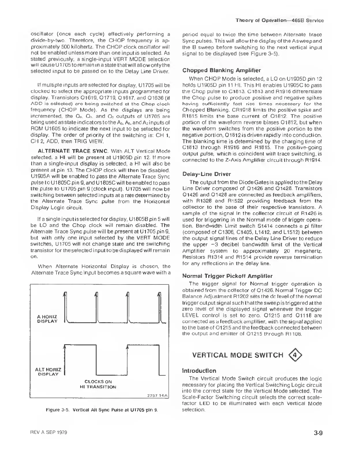
When
Alternate Horizontal
Display is
chosen,
the
Alternate Trace Sync input becomes a square
wave
with a
Figure 3-5. Vertical Alt
Sync Pulse at U1705 pin 9.
period
equal to twice the time between Alternate l race
Sync pulses. This will allow the display of the
A
sweep
and
the B sweep before switching to the next vertical input
signal
to be
displayed
(see Figure
3-5).
Chopped Blanking Amplifier
When CHOP Mode is selected, a LO on U1905D pin 12
holds
U1905D
pin 1
1 HI. This
HI
enables U1905C to pass
the Chop pulse to
C1813. C1813
and R1916 differentiate
the Chop pulse to produce positive and negative spikes
having sufficiently fast rise times necessary for the
Chopped Blanking. CR1918 limits the positive spike
and
R1815
limits
the base current of Q1812. The positive
portion of the
waveform
reverse biases Q1812, but when
the waveform switches from the
positive portion to the
negative portion.
Q1812 is driven rapidly into conduction.
The blanking time is determined by the charging time
of
C1813 through R1916 and R1815. The positive-going
output pulse, which is coincident with
trace
switching,
is
connected to the Z-Axis Amplifier circuit through R1914
Delay-Line Driver
The output from the Diode Gates
is
applied
tothe Delay
Line Driver composed of
Q1426
and
Q1428. Transistors
Q1426 and Q1428 are connected as feedback amplifiers,
with R1328 and R1522 providing
feedback from the
collector to the base of their respective transistors. A
sample of the signal in the collector circuit
of R1426 is
used for triggering in the Normal
mode of trigger opera-
tion. Bandwidth Limit switch
S1414 connects a pi filter
(composed of
C1306,
Cl
405, L1412,
and
L1512)
between
the output signal lines
of the
Delay
Line
Driver
to reduce
the upper
-3
decibel bandwidth limit
of the Vertical
Amplifier system to approximately
20
megahertz.
Resistors R1314 and
R1514
provide reverse termination
for any reflections in the delay line.
Normal Trigger
Pickoff Amplifier
The trigger signal for Normal trigger operation
is
obtained from the collector
of Q1426.
Normal
Trigger DC
Balance Adjustment R1202
sets
the
dc level of the normal
trigger output signal
such that the sweep is triggered at the
zero
level of the displayed signal whenever the trigger
LEVEL control is
set to zero. Q1215 and Q1118 are
connected as a feedback amplifier, with the signal applied
tothe
base of Ql215andthefeed back connected between
the output and emitter
of Q1215 through R1108.
VERTICAL
MODE SWITCH
Q
Introduction
The Vertical
Mode Switch circuit produces the
logic
necessary
for placing the Vertical Switching Logic circuit
into the correct
state for the Vertical Mode selected. The
Scale-Factor Switching circuit
selects the correct scale-
factor LED to
be
illuminated
with each Vertical Mode
selection.
REV
A
SEP
1979
3-9

 Loading...


