465B
Service
LIST OF
ILLUSTRATIONS
Figure
Page
1-
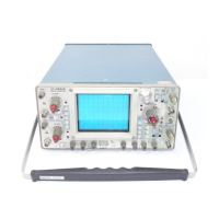
1 465B Oscilloscope
xii
2-
1 Commonly used power plugs
2-2
2-2
Regulating range selector and line fuse
2-2
2-3 Vertical
controls,
connectors, and indicators
2-3
2-4
Display controls and calibrator.
2-5
2-5
Trigger controls, connectors and
indicators 2-7
2-6
Horizontal and power connectors, controls, and indicators
2-8
2-7
Rear panel and left side panel controls, connectors, and indicators
2-9
2-8
Dimensional
drawing
2-13
2-9
Dimensional drawing (cont)
2-14
2-10 Slide-out track assemblies
2-15
2-11 Hardware
needed to mount the instrument in the
cabinet rack
2-15
2-12
Rear support kit
2-16
2-13 Installing the support block on the instrument
2-16
2-14
Methods of mounting the stationary
section to the front rails
2-17
2-15
Locating
the mounting holes for the left stationary section. Same dimensions apply to
right stationary section
2-18
2-16
Supporting the rear stationary sections: (A)
Dimensions necessary,
(B)
Completed
installation
2-19
2-
1
7 Procedure
for i nserti
ng
or removing the instrument after the slide-out tracks have
been
installed
2-20
2-18 Alignment adjustment for correct operation
2-21
2-
19 Alternative method of installing the instrument using rear support brackets
2-22
3-
1 Basic block diagram of the 465B Oscilloscope
3-1
3-2 Detailed
block diagram of
the Channel 1 Preamplifier circuit
3-4
3-3
Detailed block diagram of the Vertical
Switching Logic circuit
3-7
3-4
Switching waveform at
the junction of R1903 and R1904
3-8
3-5
Vertical
Alt
Sync Pulse at U1
705
pin
9
3-9
3-6
Detailed block diagram of the Sweep and Z-Axis Logic circuit
3-14
3-7
Detailed block diagram of the
A Sweep
Generator circuit
3-16
3-8
Detailed block diagram of the Horizontal Amplifier circuit
3-19
3-9
Detailed block
diagram
of the CRT and Z-Axis Amplifier circuit
3-21
3-10 (A) Sinusoidal sample voltage at
center
tap of
T4015.
(B)
Clamped sample voltage at
the junction of CR4111 and CR4112.
3-23
3-11
(A)
Z-Axis Amplifier
output (B)
Clamped sample voltage at the junction
of
CR4111
and
CR4112
3-24
3-12
Detailed block diagram of the Calibrator circuit
3-24
3-13
Calibrator circuit waveform diagram
3-25
3-14
Detailed block
diagram of
the Low-Voltage Power Supply circuit
3-26
3-
15 Foldover circuit action
3-27
4-
1 Typical display when high-frequency compensation is
correctly adjusted
4-35
vi
@

 Loading...