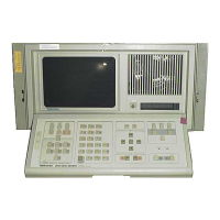
Theory of Operation-AA
501
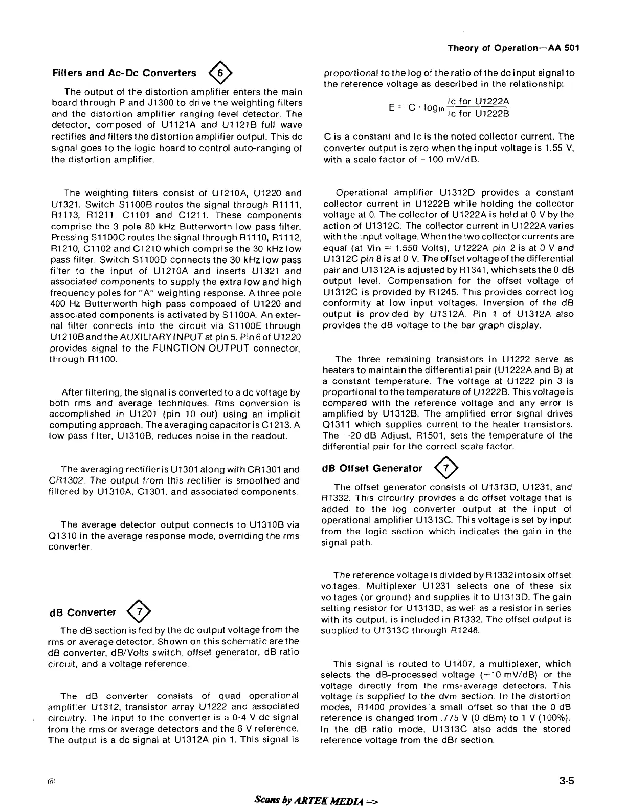
Filters and
Ac-Dc
Converters
@
The output of the distortion amplifier enters the main
board through P and
J1300 to drive the weighting filters
and the distortion amplifier ranging level detector. The
detector, composed of
U1121A and U1121B full wave
rectifies and filters the distortion amplifier output. This dc
signal goes to the logic board to control auto-ranging of
the distortion amplifier.
The weighting filters consist of
U1210A, U1220 and
U1321. Switch S1100B routes the signal through R1111,
R1113, R1211, C1101 and C1211, These components
comprise the 3 pole 80 kHz Butterworth low pass filter.
Pressing
S1100C routes the signal through R1110, R1112,
R1210, C1102 and C1210 which comprise the 30 kHz low
pass filter. Switch
S1100D connects the 30 kHz low pass
filter to the input of
U1210A and inserts U1321 and
associated components to supply the extra low and high
frequency poles for "A" weighting response. A three pole
400 Hz Butterworth high pass composed of
U1220 and
associated components is activated by
S1100A. An exter-
nal filter connects into the circuit via
S1100E through
U1210Band the AUXILIARY INPUTat pin 5. Pin
6
of U1220
provides signal to the FUNCTION OUTPUT connector,
through
R1100.
After filtering, the signal is converted to a dc voltage by
both rms and average techniques. Rms conversion is
accomplished in
U1201 (pin 10 out) using an implicit
computing approach. The averaging capacitor is
C1213. A
low pass filter,
U13106, reduces noise in the readout.
The averaging rectifier is
U1301 along with CR1301 and
CR1302. The o~ltput from this rectifier is smoothed and
filtered by
U1310A, C1301, and associated components.
The average detector output connects to
U1310B via
01310 in the average response mode, overriding the rms
converter.
dB
Converter
The dB section is fed by the dc output voltage from the
rms or average detector. Shown on this schematic are the
dB converter,
dB/Volts switch, offset generator, dB ratio
circuit, and a voltage reference.
The dB converter consists of quad operational
amplifier
U1312, transistor array U1222 and associated
circuitry. The input to the converter is
a
0-4 V dc signal
from the rms or average detectors and the
6
V reference.
The output is a dc signal at
U1312A pin 1. This signal is
proportional to the log of the ratio of the dc input signal to
the reference voltage as described in the relationship:
Ic for U1222A
E
=
C
.
loglo
Ic for U1222B
C is
a
constant and Ic is the noted collector current. The
converter output is zero when the input voltage is 1.55 V,
with a scale factor of -100
mV/dB.
Operational amplifier U1312D provides a constant
collector current in
U1222B while holding the collector
voltage at
0. The collector of U1222A is held at 0
V
by the
action of
U1312C. The collector current in U1222A varies
with the input voltage.
Whenthe two collector currentsare
equal (at Vin
=
1.550 Volts), U1222A pin 2 is at 0 V and
U1312C pin 8 is at 0 V. Theoffset voltageof thedifferential
pair and
U1312A is adjusted by Rl341, whichsetsthe0 dB
output level. Compensation for the offset voltage of
U1312C is provided by R1245. This provides correct log
conformity at low input voltages. Inversion of the dB
output is provided by
U1312A. Pin 1 of U1312A also
provides the dB voltage to the bar graph display.
The three remaining transistors in
U1222 serve as
heaters to maintain the differential pair
(U1222A and B) at
a constant temperature. The voltage at
U1222 pin 3 is
proportional to the temperature of
U1222B. This voltage is
compared with the reference voltage and any error is
amplified by
U1312B. The amplified error signal drives
01311 which supplies current to the heater transistors.
The -20 dB Adjust,
R1501, sets the temperature of the
differential pair for the correct scale factor.
dB
Offset Generator
0
The offset generator consists of U1313D, U1231, and
R1332. This circuitry provides a dc offset voltage that is
added to the log converter output at the input of
operational amplifier
U1313C. This voltage is set by input
from the logic section which indicates the gain in the
signal path.
The reference voltage is divided by
R1332intosix offset
voltages. Multiplexer
U1231 selects one of these six
voltages (or ground) and supplies it to
U1313D. The gain
setting resistor for
U1313D, as well as
a
resistor in series
with its output, is included in
R1332. The offset output is
supplied to
U1313C through R1246.
This signal is routed to U1407, a multiplexer, which
selects the dB-processed voltage
(+I0 mV/dB) or the
voltage directly from the rms-average detectors. This
voltage is supplied to the dvm section. In the distortion
modes,
R1400 provides'a small offset so that the 0 dB
reference is changed from
,775 V (0 dBm) to 1 V (lOOO/o).
In the dB ratio mode, U1313C also adds the stored
reference voltage from the
dBr section.
Scam
by
ARTEK
MEDLQ
 Loading...