102 www.xilinx.com Virtex-5 RocketIO GTP Transceiver User Guide
UG196 (v1.3) May 25, 2007
Chapter 6: GTP Transmitter (TX)
R
8B/10B Bypass
The encoder offers total control of outgoing data using the TXBYPASS8B10B signal. To
bypass the 8B/10B encoding and write the outgoing 10-bit code directly, TXBYPASS8B10B
must be driven High. While TXBYPASS8B10B is High, the TX interface for the byte is the
same as in Figure 6-2, page 92. Bypassing the encoder using TXBYPASS8B10B does not
reduce latency, but it does allow each byte of the TX interface to be bypassed individually
on a cycle-by-cycle basis.
TX Buffering, Phase Alignment, and Buffer Bypass
Overview
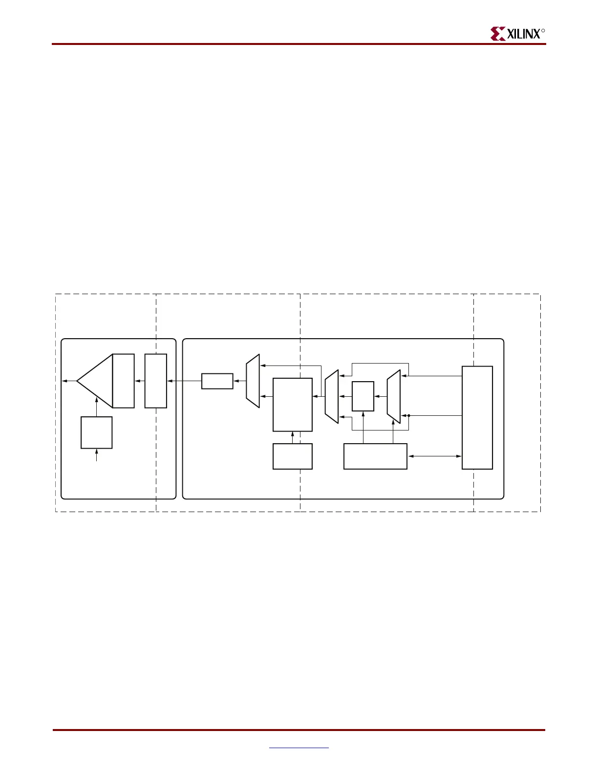
The GTP TX datapath has two internal parallel clock domains used in the PCS: the PMA
parallel clock domain (XCLK) and the TXUSRCLK domain. To transmit data, the XCLK
rate must match the TXUSRCLK rate, and all phase differences between the two domains
must be resolved. Figure 6-10 shows the XCLK and USRCLK domains.
.
The GTP transmitter includes a TX buffer and a TX phase-alignment circuit to resolve
phase differences between the PMACLK and TXUSRCLK domains. All TX datapaths must
use one of these circuits. Table 6-6 shows trade-offs between buffering and phase
alignment.
Figure 6-10: Clock Domains and Alignment Logic
TX Serial Clock
TX-PMA TX-PCS
TX
Driver
PMA
PLL
Divider
From Shared
PMA PLL
From RX
Parallel Data of
Same Channel
TX
Pre
emp
PISO
Polarity
Phase
Adjust
FIFO &
Over-
sampling
PRBS
Generate
8B
/
10B
TX PIPE Control
FPGA
Logic
PMA Parallel Clock
(XCLK)
PCS Parallel Clock
(TXUSRCLK)
FPGA
Parallel Clock
(TXUSRCLK2)
UG196_c6_10_080806
 Loading...
