Virtex-5 RocketIO GTP Transceiver User Guide www.xilinx.com 309
UG196 (v1.3) May 25, 2007
R
Appendix E
Low Latency Design
This appendix illustrates the latency of the different functional blocks inside the Transmit
and the Receive sections of the GTP transceiver.
Each functional block has a latency defined as the time difference between the inputs and
the outputs of the specific block. Some blocks in the GTP transceiver can be bypassed,
reducing the latency of the datapath through the transmitter or the receiver. The latency of
the blocks is deterministic with the exception of the RX buffer (64-element FIFO) and the
TX buffer (4-element FIFO). Bypassing buffers requires marginal conditions to be met, for
example, phase alignment procedures or USRCLK requirements.
Refer to “TX Buffering, Phase Alignment, and Buffer Bypass,” page 102, “Configurable RX
Elastic Buffer and Phase Alignment,” page 161, “Connecting TXUSRCLK and
TXUSRCLK2,” page 92, and “Connecting RXUSRCLK and RXUSRCLK2,” page 184 for the
implications and marginal conditions on bypassing buffers.
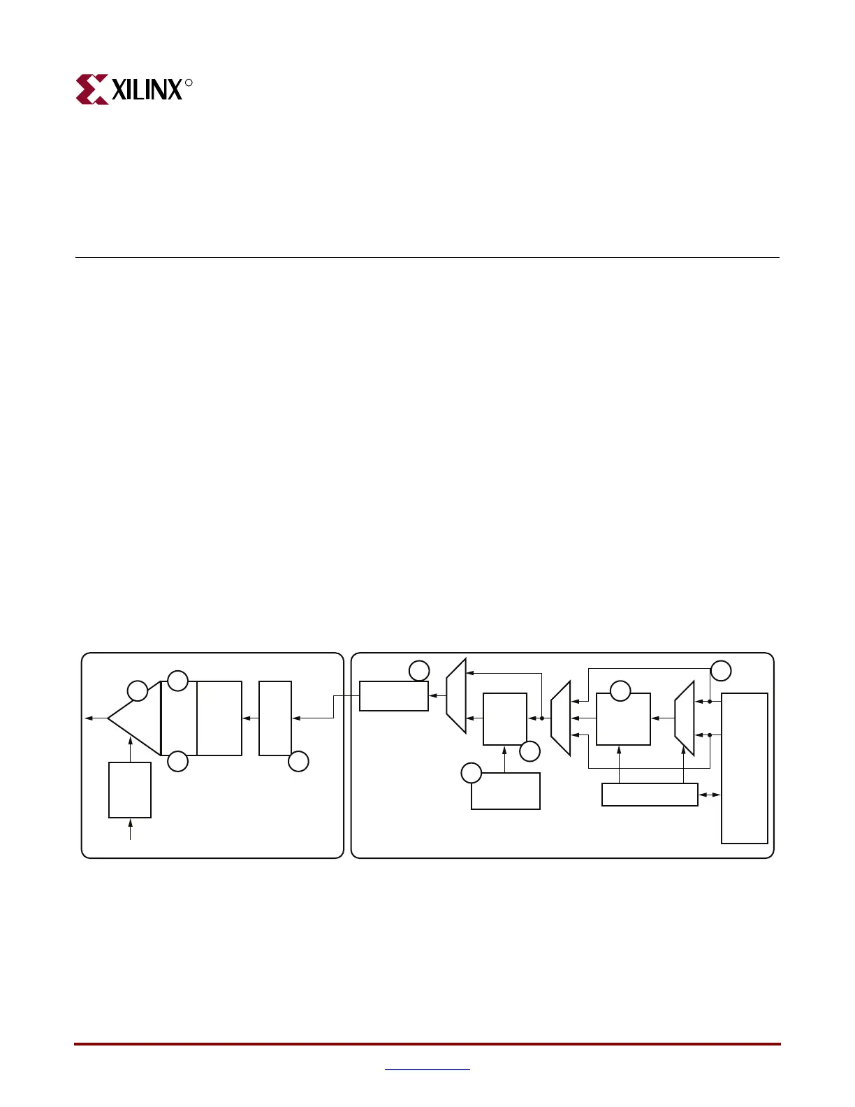
GTP Transmitter Latency
Figure E-1 shows a detailed block diagram of the GTP transmitter. Refer to Chapter 6,
“GTP Transmitter (TX),” and Figure 6-1, page 89 for more details on this figure and the
GTP transmitter blocks.
Table E-1 defines the latency for the specific functional blocks or group of functional blocks
of the transmitter section of the GTP transceiver. The values in the Block Number column
correspond to the circled numbers in Figure E-1.
Figure E-1: GTP TX Block Diagram
TX-PMA TX-PCS
TX
Driver
TX PIPE Control
From Shared PMA PLL
TX
Preemp
PISO
Phase
Adjust
FIFO
8B/10B
Encoder
FPGA
TX
Interface
Polarity
Control
PRBS
Generator
UG196_c6_01_042407
Shared
PMA
PLL
Divider
TX
OOB
&
PCI
1
2
3
5
4
7
9
68
 Loading...
