Virtex-5 RocketIO GTP Transceiver User Guide www.xilinx.com 23
UG196 (v1.3) May 25, 2007
Ports and Attributes
R
The procedures for configuring and using each of the seven major blocks in the
GTP_DUAL tile shown in Figure 1-2 are discussed in detail in the following sections:
1. “Shared PMA PLL,” page 60 (Chapter 5)
2. “Reset,” page 72 (Chapter 5)
3. “Clocking,” page 68 (Chapter 5)
4. “Power Control,” page 81 (Chapter 5)
5. “Dynamic Reconfiguration Port (DRP),” page 87 (Chapter 5)
6. “GTP Transmitter (TX),” page 89 (Chapter 6)
7. “GTP Receiver (RX),” page 123 (Chapter 7)
Ports and Attributes
This section contains alphabetical tables of pins (Table 1-2), ports (Table 1-3), and attributes
(Table 1-4) Table 1-2 lists alphabetically the signal names, directions, and descriptions of
the GTP_DUAL analog pins. Table 1-3 lists alphabetically the signal names, clock domains,
directions, and descriptions for the GTP_DUAL ports. Table 1-4 lists alphabetically the
attribute names, default values, and directions of the GTP_DUAL attributes. In all Port and
Attribute tables in this guide, names that end with 0 are for the GTP0 transceiver on the
tile, and names that end with 1 are for the GTP1 transceiver. Names that do not end with 0
or 1 are shared.
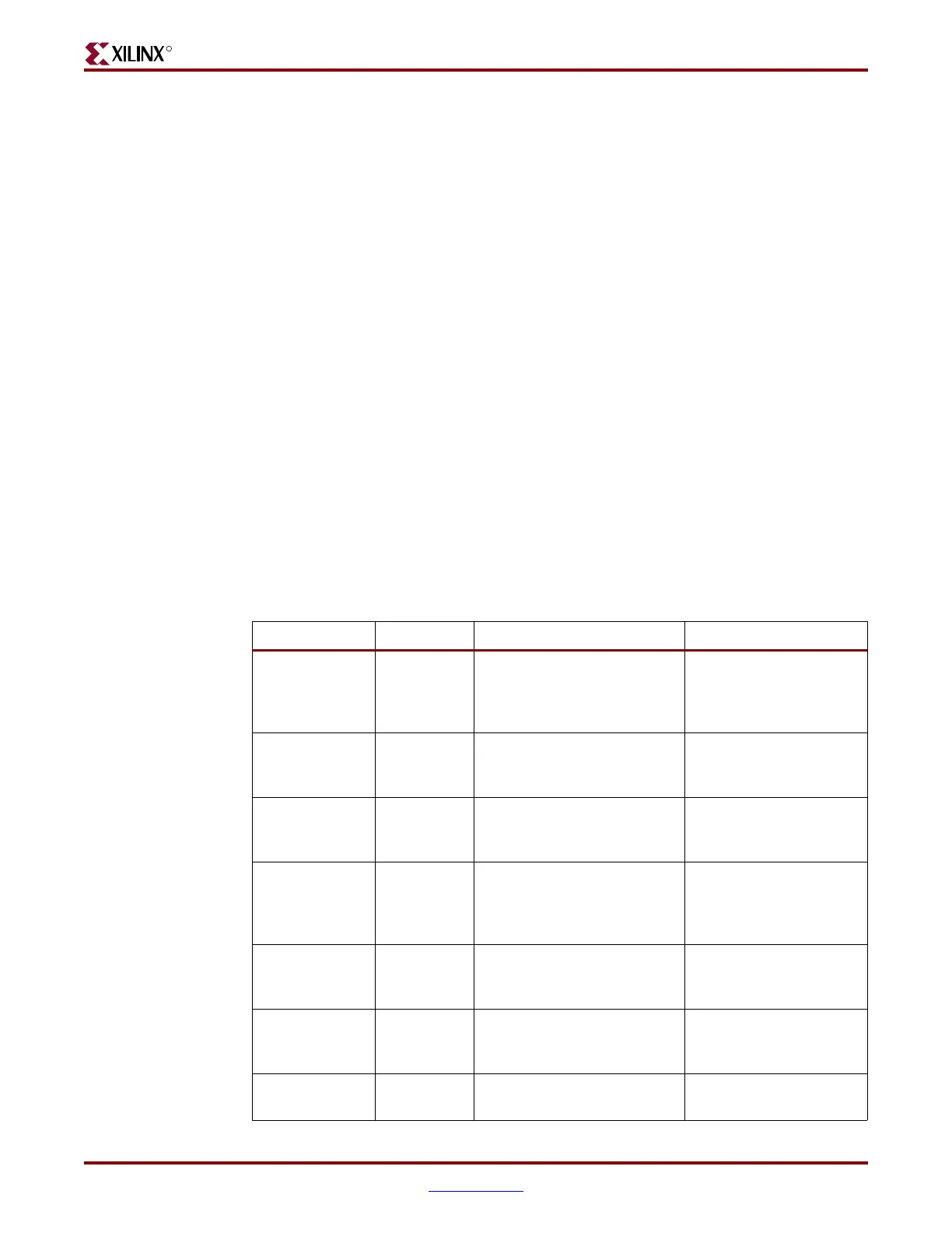
Table 1-2 summarizes all GTP_DUAL analog pins and provides links to their detailed
descriptions.
Table 1-2: GTP_DUAL Analog Pin Summary
Pin Dir Description Section (Page)
MGTAVCCPLL In
Analog supply for the shared
PLL and the clock routing and
muxing network of the
GTP_DUAL tile.
Analog Design
Guidelines (page 201)
MGTAVTTRX In
Analog supply for the receiver
circuits and termination of the
GTP_DUAL tile.
Analog Design
Guidelines (page 201)
MGTAVTTRXC In
Analog supply for resistor
calibration and standby
circuit of the entire device.
Analog Design
Guidelines (page 201)
MGTAVTTTX In
Analog supply for the
transmitter termination and
driver circuits of the
GTP_DUAL tile.
Analog Design
Guidelines (page 202)
MGTAVCC In
Analog supply for the internal
analog circuits of the
GTP_DUAL tile.
Analog Design
Guidelines (page 201)
MGTREFCLKP
MGTREFCLKN
In
Differential clock input pin
pair for the reference clock of
the GTP_DUAL tile.
Analog Design
Guidelines (page 202)
MGTRREF In
Reference resistor input for
the entire device.
Analog Design
Guidelines (page 202)
 Loading...
