EasyManua.ls Logo

Xilinx Virtex-5 RocketIO GTP User Manual

Xilinx Virtex-5 RocketIO GTP
316 pages
To Next Page IconTo Next Page
To Previous Page IconTo Previous Page
Page #70 background imageLoading...
Page #70 background image
70 www.xilinx.com Virtex-5 RocketIO GTP Transceiver User Guide
UG196 (v1.3) May 25, 2007
Chapter 5: Tile Features
R
Ports and Attributes
Table 5-4 defines the shared clocking ports.
Table 5-5 defines the shared clocking attributes.
Description
Clocking from an External Source
Each GTP_DUAL tile has a pair of dedicated pins that can be connected to an external
clock source. To use these pins, an IBUFDS primitive is instantiated. In the User
Constraints file, the IBUFDS input pins are constrained to the locations of the dedicated
clock pins for the GTP_DUAL tile. In the design, the output of the IBUFDS is connected to
the CLKIN port. The locations of the dedicated pins for all the GTP_DUAL tiles are
documented in Chapter 4, “Implementation.” Chapter 10, “GTP-to-Board Interface”
provides a selection of suitable external oscillators and describes the board-level
requirements for the dedicated reference clock. Figure 5-4 shows a differential GTP clock
pin pair sourced by an external oscillator on the board. Refer to Chapter 10, “GTP-to-Board
Interface,” REFCLK Guidelines for IBUFDS details.
Table 5-4: Shared Clocking Ports
Port Dir Clock Domain Description
CLKIN In N/A Reference clock input to the shared PMA PLL.
REFCLKOUT Out N/A
The REFCLKOUT port from each GTP_DUAL
tile provides access to the reference clock
provided to the shared PLL (CLKIN). It can be
routed for use in the FPGA logic.
Table 5-5: Shared Clocking Attributes
Attribute Description
CLK25_DIVIDER
The internal digital logic for GTP_DUAL tile management runs at about
25 MHz. CLK25_DIVIDER is set to get an internal clock for the tile.
1: CLKIN <
25 MHz
2: 25 MHz < CLKIN <
50 MHz
3: 50 MHz < CLKIN <
75 MHz
4: 75 MHz < CLKIN <
100 MHz
5: 100 MHz < CLKIN <
125 MHz
6: 125 MHz < CLKIN <
150 MHz
10: 150 MHz < CLKIN <
250 MHz
12: CLKIN > 250 MHz
CLKINDC_B
Must be set to TRUE. Oscillators driving the dedicated reference clock
inputs must be AC coupled.
Figure 5-4: Single GTP_DUAL Tile Clocked Externally
GTP_DUAL
MGTREFCLKP
IBUFDS
MGTREFCLKN
CLKIN
UG196_c5_04_110306

Table of Contents

Question and Answer IconNeed help?

Do you have a question about the Xilinx Virtex-5 RocketIO GTP and is the answer not in the manual?

Xilinx Virtex-5 RocketIO GTP Specifications

General IconGeneral
BrandXilinx
ModelVirtex-5 RocketIO GTP
CategoryTransceiver
LanguageEnglish

Summary

Revision History

About This Document

Section 1: FPGA Level Design

Chapter 1: Introduction to the RocketIO GTP Transceiver

GTP Transceiver Overview

Introduces the Virtex-5 RocketIO GTP transceiver and its features.

Chapter 2: RocketIO GTP Transceiver Wizard

GTP Transceiver Wizard Usage

Details on using the RocketIO GTP Transceiver Wizard for wrapper generation.

Chapter 3: Simulation

Simulation Overview

Covers prerequisites and environment setup for simulating GTP transceiver designs.

Simulation Ports and Attributes

Details simulation-only ports and attributes for the GTP_DUAL tile.

Simulation SmartModel Attributes

Explains attributes controlling SmartModel behavior for simulation accuracy.

Chapter 4: Implementation

Implementation Overview

Provides information on mapping GTP_DUAL tiles to device resources and package combinations.

Implementation Description

Explains GTP_DUAL tile positioning and UCF creation methods.

GTP_DUAL Package Placement

Illustrates GTP_DUAL placement for various packages and nomenclature.

Chapter 5: Tile Features

GTP Tile Features Overview

Overview of shared GTP functions for power, clocking, resets, and reconfiguration.

Shared PMA PLL Overview

Describes the shared PMA PLL used for generating high-speed serial clocks.

GTP Clocking Overview

Explains methods for driving the CLKIN port for GTP transceivers.

GTP Reset Overview

Details the three ways to reset a GTP_DUAL tile and its subcomponents.

GTP Power Control Overview

Discusses power control modes for generic and protocol-specific power management.

DRP Overview

Explains the DRP interface for dynamic parameter changes of the GTP_DUAL tile.

Chapter 6: GTP Transmitter (TX)

GTP Transmitter Overview

Overview of the GTP transmitter, including PCS and PMA blocks.

FPGA TX Interface Details

Describes the interface for transmitting parallel data to the GTP transceiver.

8B/10B Encoder Functionality

Details the 8B/10B encoder for outgoing data, its benefits, and costs.

TX Buffering and Phase Alignment Overview

Explains TX buffer, phase alignment, and bypass options to resolve clock domain differences.

Chapter 7: GTP Receiver (RX)

GTP Receiver Overview

Overview of the GTP receiver, including PCS and PMA blocks.

RX Termination and Equalization Details

Details circuits for optimizing termination and compensating for high-frequency losses.

RX Clock Data Recovery Details

Describes the CDR circuit's function in recovering the clock from incoming serial data.

Comma Alignment and Detection Details

Details the alignment block for aligning specific commas to byte boundaries.

Chapter 8: Cyclic Redundancy Check (CRC)

CRC Block Overview

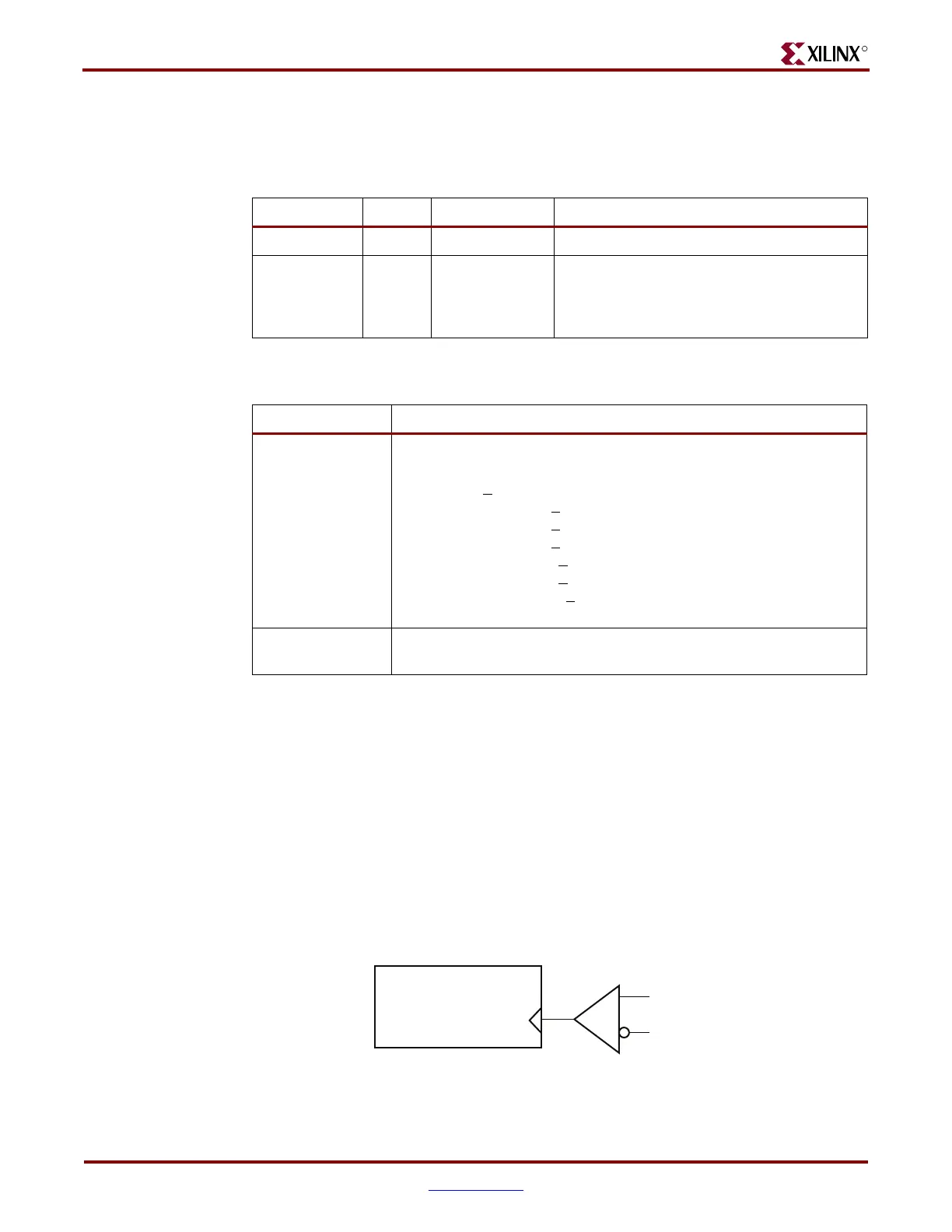
Shows the basic port interface and operation of the CRC block.

CRC for Error Checking

Explains how CRC is used as an error-checking mechanism for data frames.

CRC Primitive Details

Describes the CRC32 and CRC64 primitives used for CRC calculation.

Chapter 9: Loopback

Loopback Modes Explained

Explains loopback modes and their categories: near-end and far-end.

Loopback Configuration Ports and Attributes

Defines the ports and attributes for configuring loopback modes.

Near-End PMA Loopback Mode

Details Near-End PMA loopback mode using the Near-End source for data generation.

Chapter 10: GTP-to-Board Interface

Analog Design Guidelines for GTP

Discusses power supply and clocking design guidelines for overall system performance.

REFCLK Selection Guidelines

Focuses on selecting the reference clock source or oscillator based on characteristics.

SelectIO Crosstalk Guidelines for GTP

Provides guidelines for SelectIO usage to minimize impact on GTP transceiver performance.

Chapter 11: Design Constraints Overview

Physical Interconnect Topology Overview

Defines a physical link between transceivers as a channel.

PCB Materials and Traces Overview

Discusses PCB materials and trace design for optimal performance.

Powering Transceivers Overview

Discusses power supply designs for transceivers to achieve low link error rates.

Chapter 12: PCB Materials and Traces

Dielectric Losses

Discusses signal energy loss due to dielectric characteristics.

Choosing the Substrate Material

Provides guidance on selecting substrate materials for performance and cost.

Trace Routing

Provides guidelines for routing high-speed differential traces.

Chapter 13: Design of Transitions

Excess Capacitance and Inductance

Discusses excess capacitance and inductance in differential transitions.

Time Domain Reflectometry (TDR)

Explains TDR techniques for identifying transition issues.

Differential Vias

Explains the common transition type for differential signals using GSSG vias.

Chapter 14: Guidelines and Examples

Summary of Guidelines

Provides a quick reference to guidelines and strategies for high-speed serial channels.

BGA Escape Example

Illustrates routing transceiver signal pairs along BGA edges.

Section 3: Appendices

MGT to GTP Transceiver Design Migration

Describes differences migrating from Virtex-II Pro/Virtex-4 MGTs to Virtex-5 GTP transceivers.

OOB/Beacon Signaling

Provides support for Out-of-Band (OOB) signaling for SATA and beaconing.

8B/10B Valid Characters

Lists valid Data characters and K characters for 8B/10B encoding.

DRP Address Map of the GTP_DUAL Tile

Lists attributes and their mappings to DRP addresses and bit locations.

Low Latency Design

Illustrates the latency of functional blocks within the Transmit and Receive sections.

Related product manuals