Virtex-5 RocketIO GTP Transceiver User Guide www.xilinx.com 229
UG196 (v1.3) May 25, 2007
Coupling
R
Plugging these values into Equation 11-4 gives:
Equation 11-5
Equation 11-4 is only valid for cases where the problem data pattern consists of a single
sequence of consecutive identical digits. More complex pathological cases can occur in
protocols using block coding schemes and scrambling.
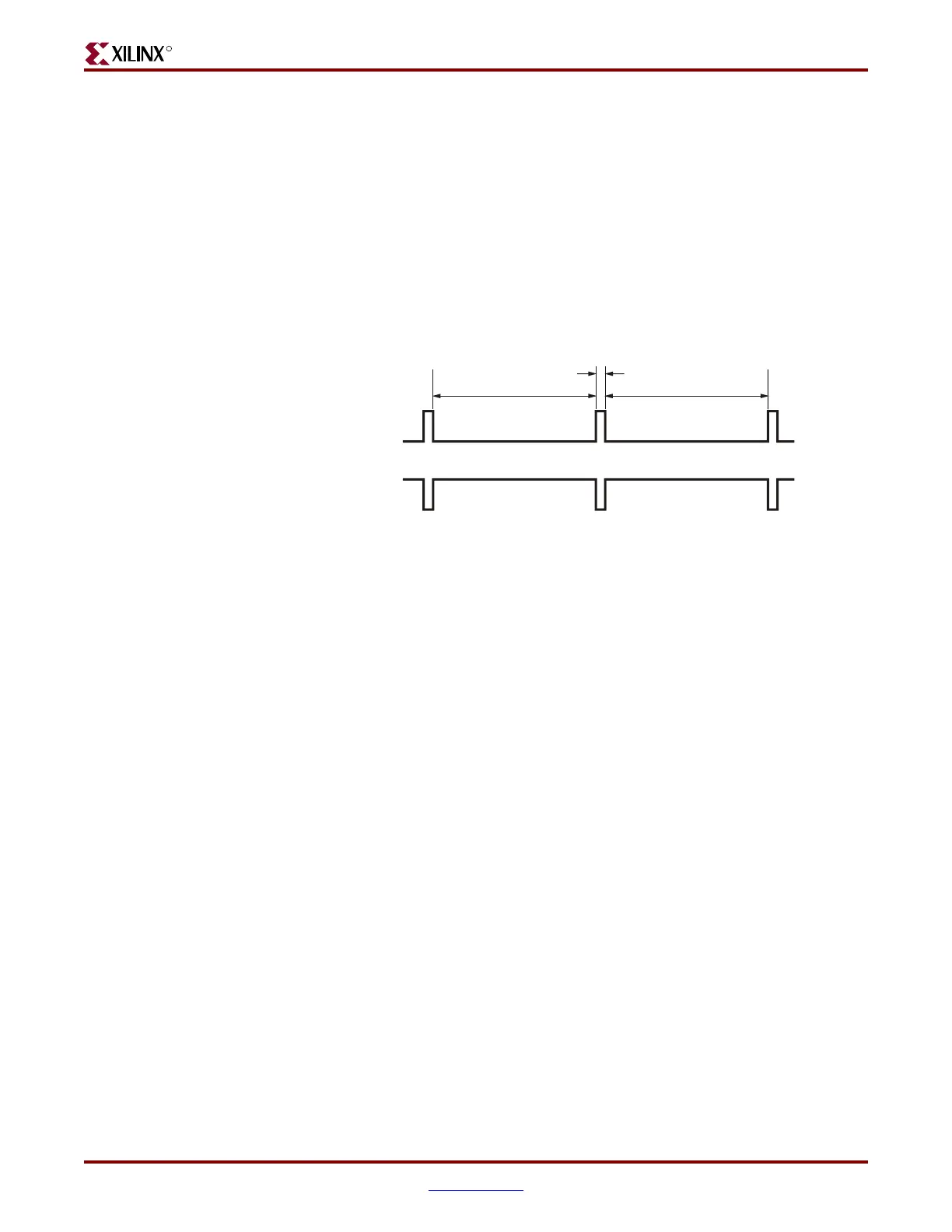
One example of such a case occurs in the serial digital interface (SDI) used to transmit
digital video. Figure 11-6 illustrates this pattern, which is called an equalization test
pattern.
The waveform is 20 bits long and consists of a single “1” bit followed by 19 “0” bits. The
complementary waveform, a single “0” bit followed by 19 “1” bits is also equally likely.
The EQ waveform can repeat across the entire length of the active portion of a video line.
For standard definition video (SD-SDI), this can consist of up to 720 consecutive repetitions
of the 20-bit pattern. For high definition video (HD-SDI), this pattern can repeat up to 1920
consecutive times.
For this case, the blocking capacitor value cannot be calculated using Equation 11-4
because an N
CID
value of 19 does not reflect the total time that a DC imbalance is being
applied on the line. To properly analyze charge accumulation on blocking capacitors for
this case, more extensive analysis beyond the scope of this document is required.
SelectIO to Serial Transceiver Crosstalk Guidelines
The breakout of SelectIO signals adjacent to transceiver analog supply pins and REFCLK
pins are also important. As noted in “SelectIO-to-GTP Crosstalk Guidelines,” page 216,
these SelectIO requirements, if not taken into consideration, can have an effect on
transceiver performance. This impact occurs when SelectIO solder balls are adjacent to
transceiver analog supply or REFCLK solder balls and their corresponding PCB vias are
adjacent as well, creating both package and board coupling mechanisms. The solder balls,
which are part of the package, offer some coupling, and the adjacent PCB vias offer two to
four times more coupling. Simulation suggests that the amount of coupling due to adjacent
PCB vias is affected by which layer the SelectIO escape is located and on how the analog
supplies are delivered to the transceivers. Simulation predicts that coupling can be
reduced by using the upper PCB routing layers to route SelectIO signals and/or by using
a higher layer to distribute transceiver analog power supplies. When a design dictates that
SelectIO signals with BGA adjacency to transceiver analog supply pins are to be used for
high-drive/high-speed applications, the following guidelines apply:
Figure 11-6: SDI EQ Pathological Waveform
C
3.20 10
10–
×()– 5×
275× 1
1.2 3.20 10
12–
×()
6.40 10
11–
×
-------------------------------------------–
⎝⎠
⎜⎟
⎛⎞
ln×
-------------------------------------------------------------------------------------
0.17nF==
19 "0"s
one "1"
UG196_c11_06_091906
19 "0"s
EQ Patterns
 Loading...
