230 www.xilinx.com Virtex-5 RocketIO GTP Transceiver User Guide
UG196 (v1.3) May 25, 2007
Chapter 11: Design Constraints Overview
R
• Apply power to the transceiver analog supplies with a plane or wide buses a few
layers below the top of the board. Using a blind via to the transceiver analog supplies
is better than using a through via. Shield the supply plane with GND planes above
and below.
• If a through via to supply the transceiver analog supply pins must be used, use an
upper layer to supply analog power to these vias. Route SelectIO nets in the
uppermost layer available after transceiver signal and transceiver analog supply
routing is implemented.
• If supplying transceiver power from the bottom of the board, route these SelectIO nets
in the highest available routing layer.
• Do not use SelectIO blocks adjacent to REFCLK pins because the REFCLK pins are a
reference clock source to the transceivers either in the same tile or in other tiles.
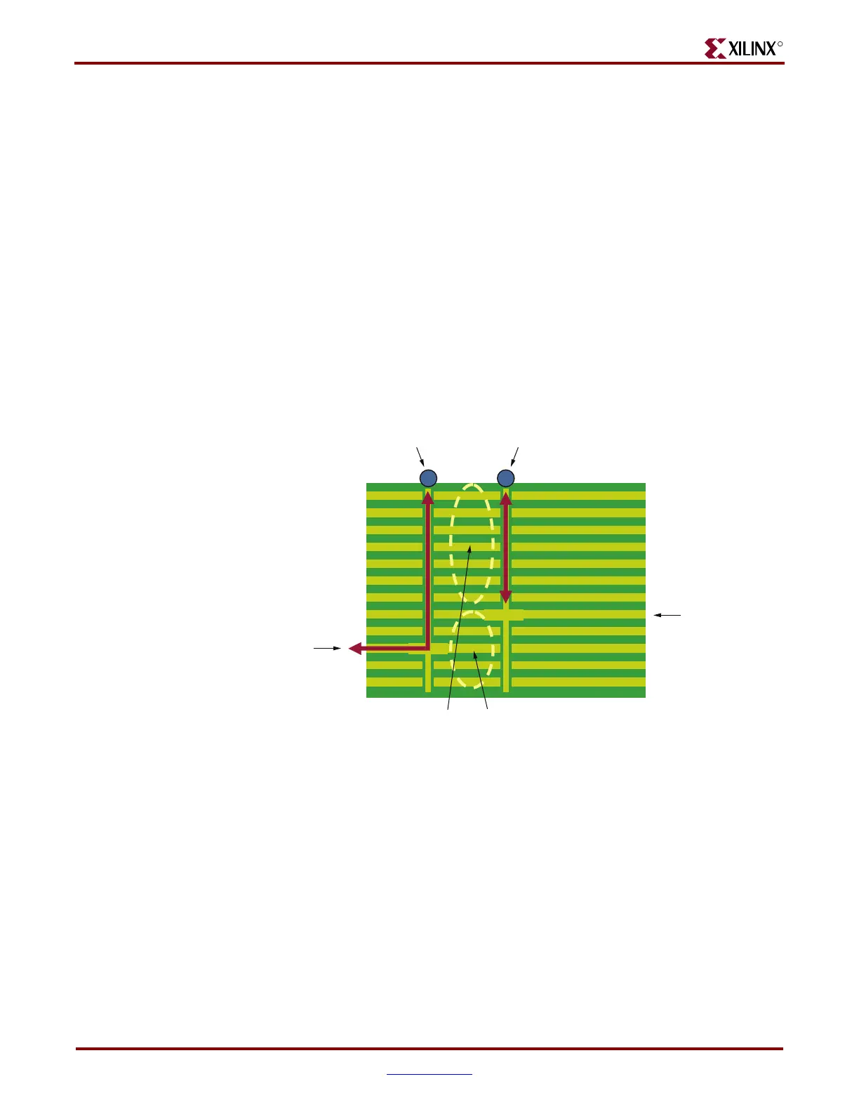
Figure 11-7 depicts the coupling regions for BGA adjacent SelectIO signals. The primary
coupling mechanism is mutual inductive coupling, which occurs in the area between the
active signal path and the power via. The secondary coupling mechanism, also shown in
Figure 11-7, is capacitive. The primary coupling mechanism is much larger, and the
recommendations are designed to minimize this effect.
Figure 11-7: Via Structures for BGA Adjacent SelectIO Signals
RocketIO power pinSelectIO signal
RocketIO
power plane
SelectIO
signal path
Capacitive coupling in this area
to power “via stub” (secondary)
Mutual inductive coupling in
this area between active signal
path and power via (primary)
UG196_c11_07_013007
 Loading...
